Doctoral Dissertation
Scalable photonics in SiC
Scalable photonics are necessary for large scale on chip use of single defects.
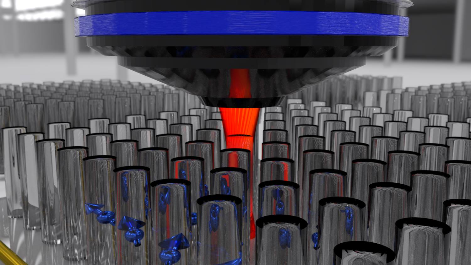
Figure 4.1: Nano pillar array. with embedded spin defects and optical excitation and detection. From ref. (Radulaski et al., 2017).
The presented results in the following chapter were achieved by an international collaboration with the group of Prof. Jelena Vučković in Stanford University (USA) and published in
M. Radulaski & M. Widmann, M. Niethammer, J. Wrachtrup, et al., Scalable Quantum Photonics with Single Color Centers in Silicon Carbide, Nano Lett. 17 (2017) 2-6. (Radulaski et al., 2017)
Introduction
Interfacing single photon emitters to optical fibers is a demanding goal for practical use not only for nanoscale sensor technologies but also for qip purposes. Atomic scale defects in solids show good potential for sensors and applications in qip. It was demonstrated that SiC is such a solid, serving as a platform for single photon emitters with electron spins and allowing quantum operations at room temperature. Motivated by the presented long coherence time in the ms range (see Chapter 3 and (Christle et al., 2015; Simin et al., 2017; Widmann et al., 2015)) spin defects in SiC show promises for their usage as quantum bits and for sensitive and precise sensors (Niethammer et al., 2016) for various observables such as temperature and electric (Falk et al., 2014) and magnetic fields (Niethammer et al., 2016). The sensitivity for magnetic fields for spin defects is given by (Balasubramanian et al., 2008), with the line width of the spin signal, the detection efficiency, the photon emission rate and the measurement time. Hence, the sensors sensitivity is proportional to the square root of the signal strength, which is composed of both spin contrast and light intensity. Therefore, any increase of these values is a important issue. That improvement is in particular necessary for the , as both the quantum yield and the spin contrast of 4% is low compared to other spin systems, eg. the NV in diamond where spin contrast of 30% for single NVs in bulk crystal are routinely achieved.
In a recently published paper, it was demonstrated that the spin contrast for an ensemble can be over 100% at low temperature (Nagy et al., 2018b). For the other parameter, an improvement in detection efficiency can be achieved by fabricating a sil into the crystal. It was already shown in Section sil that the collection efficiency can be increased by a factor of three by using a sil. However the sils are typically created by focused ion beam techniques, as demonstrated in Chapter 2. By considering the time effort for creating a single sil, which is in the order of hours (Widmann et al., 2015), a large scale production is costly and only practicable for research purposes. Hence, one important step towards wafer-scale sensor production is to create large arrays of photonic structures simultaneously. Before coming to the experimental results, the theoretical background shall be set for the engineering and characterization of photonic waveguides. Next, numerical simulations for optimizing the geometrical structure of the waveguide for enhanced collection efficiency will be presented. That is followed by a brief presentation of the technique for patterning such light-guiding channels in SiC through a photo-lithographic techniques performed by M. Radulaski and coworkers in Stanford. Then the experimental results on the enhanced optical properties of the embedded defects will be shown, and the comparison to the previously discussed numerical simulations will be performed. The chapter concludes with a brief outlook towards for next generation photonic structures and their potential applications.
Theory
Pillar As a Step Index Fiber
The nano-pillar structure presented in this chapter acts as a waveguide for the embedded defect, where the defect is modeled as a dipole emitter. Basically, a waveguide is a step index fiber with a core having a higher refractive index and a cladding with a lower refractive index (which is air here). Light is here confined based on total internal reflection. Total internal reflection is occurs only when the angle between the fiber normal and the incoming light is smaller than . The fiber can support various optical modes which are formed depending on both refractive indices and their respective radii and .

Figure 4.2: Step index fiber schematic. with a core and cladding and their respective radii and and refractive indexes and
For simplicity, the light emitted by the quantum emitter is assumed to be monochromatic with a wavelength (Mitschke, 2010). The electric and magnetic fields of a light field obey the wave equation . For the fiber geometry, it is convenient to transform it to cylindrical coordinates . The wave equation can be written as:
(4.1)
, where with as positive and negative integer numbers and the propagation constant along . The equation Equation 4.1 reads then as:
(4.2)
Two types of modes are possible, guided and radiative ones. Guided modes are allowed only when and , with discrete values of . Hence one defines the transversal components of the wave numbers in the core and cladding (Mitschke, 2010):
where defines the radial phase constant and defines the transverse decay constant of the amplitude. Equation 4.2 can then be split into core and cladding part:
The solutions for these differential equations are given by Bessel function of the first kind and modified Bessel function of the second kind :
With transversal standing waves inside the core, which are described by and decaying waves in the cladding described by . The constants and are a measure how is changed in the cladding and core. If is large, the radial distribution in the core exhibits more oscillations and if is large the penetration into the cladding is small as decays rapidly.
Another important value for a fiber is the acceptance angle between the fibers axial direction and the coupled light, which is defined by (Mitschke, 2010):
(4.3)
where the argument of is commonly known as the na. Hence, the na for a fiber is given by:
(4.4)
It is a common practice to multiply Equation 4.3 with the radius to obtain a normalized frequency, which is often called the number and is defined (Mitschke, 2010) as:
which contains all relevant information. For each possible guided mode there exists one value of where the mode cannot be guided any more. A particular fiber with a parameter smaller than 2.405 called single-mode fiber (Mitschke, 2010), as only one mode can exist. The shape of the mode is Gaussian distributed and has the maximized intensity at the center of the core. It is possible for any fiber to calculate cutoff wavelength (or frequency) from , below only one solution exists where above multiple modes are allowed.
Quantum Emitters Embedded In a Fiber
Quantum emitters in a pillar can be modeled as an electric dipole with a connected dipole moment oscillating with a frequency at a position within a fiber (Henderson et al., 2011). The resulting polarization density of a single dipole is given by . By summing all the power captured into all guided and radiative modes the total polarization density is then given by:
(4.5)
where subscript stands for discrete guided modes and stands for radiative modes. is defined as and the integration is necessary due to the continuous nature of the -values (Henderson et al., 2011). By calculating the emitted power as given in Equation 4.5 one can find that the dipole emission is altered due to the creation of a cavity effect which is caused by the core-cladding interface. Conclusively the dipole emission is altered, which leads to constructive and destructive interference effects. These effects can be seen when the intensity is plotted as a function of the core diameter, which will be presented in the following fdtd simulation and experiment.
FDTD modeling
fdtd is a numerical simulation method used to solve time dependent Maxwell equations and goes back to K.Yee (Yee, 1966). He found a convenient way to solve these equations, as the numerical curl can become complicated to calculate when all three spatial dimensions are considered. As for any numerical calculation, the equations are discretized to the spatial and time grids to approximate partial derivatives. However, the electric and magnetic-fields are not calculated at the same Cartesian point, but are calculated in a alternating manner in both space and time using leapfrog algorithm, explained as follows. First, the components of the electric field vector are solved at given time point. Next, the corresponding components of the magnetic field at the next time point are calculated using the previously calculated electric and magnetic field components. This process is repeated to simulate wave propagation. The time stepping scheme further avoids the complexity for solving Maxwell’s equations simultaneously for both electric and magnetic fields. This algorithm is the core of any fdtd methods and has been applied to various photonic applications.
Simulation results
The light emission of a color center, which is placed inside a pillar structure was simulated by fdtd methods. The refraction index distribution follows the simple geometrical form of a pillar obeying cylindrical symmetry with a radius and an extension in . The height of the pillar is fixed to 400 nm, whereas the diameter is variated over a range of 400 nm to 1400 nm with a step size of 50 nm.
The color center, essentially a dipole emitting at around 916 nm, is located at with and . The color center is assumed to be resonantly excited at the zpl via cw laser excitation, which is centrally aligned in respect to the cylinder (). Because the sample used in the experiments was grown 4-degree off from z-axis, the orientation of the dipole in the simulation was also tilted by 4°. Hence the total collected electric field is composed of:
where and are the electric field components in radial and axial directions, respectively. Those components are shown in terms of collection efficiency in Figure 4.3a.

Figure 4.3: Simulated collection efficiency and electric field propagation. of a dipole inside a pillar ((a)-(c), and (e)) and inside bulk (d) (a) Calculated collection efficiency and electric field components as a function of the pillar diameter . Red line shows the efficiency of a 4° tilted dipole, whereas the radial/axial component is plotted by blue/orange lines, respectively. (b) fdtd simulation result of electric field propagation from a dipole inside a pillar. Dipole is located at the center of a pillar with a fixed diameter 600 nm (c) Calculated far field emission patterns from (b). (d) Calculated collection efficiency as a function of the depth of an dipole emitter in a bulk SiC crystal, with the same coloring as in (a). (e) Collection efficiency for a dipole located at the center of the pillar (blue line) and at optimized positions (red line) and for a dipole in bulk (black line). All simulations in this figure were performed by M. Radulaski and reprinted with permission from ref. (Radulaski et al., 2017).
The collected light emission is evaluated by a two-step analysis. In the first steps, the power of the emitted light which penetrates the walls of the simulation space is monitored. Then, the light fraction which is guided upwards along -direction is calculated, and the result is plotted in Figure 4.3b.
The next step is to analyze the far field emission patterns, which are plotted in Figure 4.3c. Based on the far fields emission pattern, the light component in axial direction is collected by a given na. As seen in Figure 4.3a the axial dipole component has the main contribution to the total power fraction. Because of that, the radial emission component is neglected for further analysis.
Influencing Factors on The Collection Efficiency
The Dipole Position
In order to quantify the influence of centers position inside a pillar on the collection efficiency, the dipole location was varied in radial and axial direction. As above mentioned, the contribution from radial emission can be neglected. Hence only the axial component is analyzed.

Figure 4.4: Dipole position dependence of collection efficiency. for various pillar diameter (color coded) (a) Collection efficiency as a function of axial position of a dipole with a fixed with radial location () inside the pillar. (b) Collection efficiency as a function of the dipoles radial position with a fixed axial location ( 400 nm) inside the pillar. From ref. (Radulaski et al., 2017).
The simulation result, plotted in Figure 4.4a, shows a maximized collection efficiency when the emitter is placed at the bottom of the pillar. That is an indication that the pillar acts as a waveguide, which is more efficient when the axial length has a sufficient length. In addition, as shown in Figure 4.4b, the collection is maximized for diameter sizes when the dipole is placed exactly in the pillars center at . The efficiency drops drastically as the offset in radial direction. The optimum position of a defect in a 600 nm tall pillar is at (0,0) position yielding a maximized collection efficiency of about 25%.
Furthermore, it was found that the collection efficiency can be increased even more by using a higher na objective. In comparison to the lower na objective, the gain can be up to a factor of two.
Pillar Fabrication Process

Figure 4.5: Lithographic process. From ref. (Radulaski et al., 2017).
The fabrication of the presented nano pillars is based on an electron-beam lithography technique, widely used in research. Electron-beam lithography is regarded as non-scalable technique in industry because beam scanning is time consuming and thus it is costly. A good news is that pillar structures with a diameter of few hundreds of nanometers can probably be fabricated using photolithography.
The pillar fabrication was performed by M. Radulaski and coworkers in Stanford, and the process is illustrated in Figure 4.5. The first step is the creation of in a high purity semi-insulating 4H-SiC sample. As for the studies presented before, the sample was irradiated at room temperature with 2 MeV electrons with a fluence of cm which allows for defect densities of about cm (see Figure X771dose in Section engsingle). The second step is to deposit a hard etch mask on the sample surface. This was achieved by aluminum evaporation which coats the surface with a layer of 300 nm. The third step is the resist sputter process. There a MICROPOSIT ma-N negative tone resist was used for the subsequent patterning of the pillars. The patterning was then achieved by an electron-beam lithography system running at 100 keV (JEOL JBX-6300FS). The pattern was then transferred to the hard mask by a mixture of and plasma using an icp metal etcher (Plasma Therm Versaline). The next pattern transfer to the SiC crystal was achieved by in the same etcher. To remove the remaining mask a metal etching process in a bath of an aluminum etch was used and is the final step of the fabrication process.

Figure 4.6: SiC nano pillar SEM-images. (a) multiple pattern of nano pillars with un-etched bulk areas at the bottom. (b) Closeup of a nano-pillar. (c) Tilted closeup image from a pillar patch. Scans performed by M. Radulaski and reprinted with permission from ref. (Radulaski et al., 2017).
The fabricated pattern is composed of multiple arrays of pillar patches. Each patch counts 10x10 nano-pillars with variable diameters ranging from 400 nm to 1200 nm as illustrated in the sem image shown in Figure 4.6a. A close-up image is presented in Figure 4.6b where the profile of the pillars is shown. The pillars have heights of 800 nm where the top is tapered to a cone, which reduces the diameter by 120 nm.
Experimental Results
The pillar structure was mounted on a confocal laser microscope (see Section setup) to investigate incorporated in the pillars. A confocal raster scan is presented in Figure 4.7a.

Figure 4.7: Experimental results. (a) PL Confocal raster scan of a pillar patch. (b) PL intensity of a single plotted as a function of the optical power, saturating at 22 kcps. The red line indicates a fit to the data. (c) Countrate as a function of the pillar diameter. (d) PL spectrum at room temperature of a single emitter in a nanopillar. (e) Typical second order correlation function. Clear visible anti-bunching at zero time delay between photon arrivals, a unambiguous evidence for single photon emission. The red line shows a double exponential fit to the data. (f) odmr signal from a single in a nanopillar. The red line shows a Lorentzian fit to the data. From ref. (Radulaski et al., 2017).
The scan reveals one pillar patch with some pillars hosting color centers. The enhanced photon count rate is confirmed by saturation measurements illustrated in Figure 4.7b. The saturated count rate was specified to 22 kcps. The background luminescence was determined by collecting the light from a pillar without a color center. For each found center a saturation curve was measured and fitted. For more details see Equation sat.
The saturation curve and the fitting was tested on more than 50 emitter for various pillar diameters. The saturated count rate PL was then determined from the least-square fits and is plotted in Figure 4.7c. From the plot the optimum pillar diameter is found at around 600 nm, which is in a well agreement with the results from the simulation shown in Figure 4.3. The maximum detected photons per second was found within the 600 nm diameter pillars and determined to 22 kcps. From the comparison between the fdtd-calculation and the experimental data, clearly the revival at 1000 nm is resembled as well. The large variations in the collection efficiency within the same pillar diameter is very well explained by the particular location of the color defect in the pillar. As explained in Section 4.3.1.1 the efficiency is strongly dependent on the dipole position.
A typical room temperature PL-spectrum is shown in Figure 4.7d. Similar to the spectra shown in Figure correlationSil in Chapter 2 the zpl is not visible at room temperature. In order to check if the color centers are true single quantum emitters second order correlation measurement as introduced in Section Experimental realization was performed. Clearly, these found color centers are single emitters as the anti-bunching, well below 0.5, is observed at zero time delay. The final evidence that the incorporated color centers are indeed centers is then unambiguously given by spin resonance test. A typical odmr experiment is presented in Figure 4.7f. By analyzing the odmr-spectrum which reveals the known fine-structure originated by a residual magnetic field.
Conclusion and Outlook
In this chapter it has been demonstrated that SiC photonic structures with embedded color centers can be fabricated in a scalable context. The color centers were introduced by electron irradiation with energies of 2 MeV and a dose of 1E14 cm. A subsequent standard lithographic process formed 800 nm-tall nanopillars. In one lithographic run pillars with diameter sets of 400 nm to 1400 nm were produced in order to investigate the optimized conditions for the best collection efficiency. The best collection efficiency, up to 22 kcps was found at diameters of 600 nm. That result is in a good agreement to the fdtd-simulations and also with the theoretical prediction in (Henderson et al., 2011). To test if the color centers remain as single photon sources after the harsh fabrication process measurements was performed. To further prove that the embedded color centers are indeed centers single spin resonance was successfully demonstrated.
The fabrication of nano-scale structures with single spin defects paves the way for future waver scale SiC-quantum applications as demonstrated for color centers in diamond. There, similar nano-fabrication techniques have led to equivalent photonic components, such as waveguides, photonic crystals and optical nanoresonators. Moreover, diamond nano pillars with embedded NVs were mounted on nanoscale cantilevers, providing means for high sensitivity in detecting nano-mechanical motions in force microscopy (Kleinlein et al., 2016).
To extend the capabilities, another prospect relies on the coupling of the light mode into a fiber. Here optical modes are coupled into nano-objectives fabricated by two-photon direct laser writing methods (Gissibl et al., 2016), mounted on the fiber tip. Similar approaches have been successfully applied to quantum dots (Fischbach et al., 2017).