Doctoral Dissertation
Electrically and optically driven single photon emitters in SiC
Figure 7.1: A SiC quantum light emitting pin diode. as an artistic impression.
The presented results in the following chapter were achieved by an international collaboration with the National Institutes for Quantum and Radiological Science and Technology, published in M.Widmann, M. Niethammer, T. Makino, T. Rendler, S. Lasse, T. Ohshima, J. Ul Hassan., N. T. Son, S.-Y. Lee, J. Wrachtrup, Bright single photon sources in lateral silicon carbide light emitting diodes, Appl. Phys. Lett. 8 (2018) 9. (Widmann et al., 2018a)
Introduction
Single-photon sources are regarded as an important building block for applications of quantum information and communication. These sources make it possible to send quantum information with these photons over long distances. The quantum information can be impressed on the photon by polarization. Furthermore, the photons thus generated can be entangled, either via the same source or another source. In the former case, a photon is delayed to be entangled at the same time with another photon from the same source. In the latter case, the entanglement between photons from two different sources is achieved, with the condition that the emitted photons have the same frequency. The generation of single photons can be realized with, for example, optically pumped quantum dots (Michler et al., 2000). However, also individual defects in solids can be used similarly, and thus the silicon vacancy as a single photon source presented in this work.
The semiconductor device structure presented in this chapter was designed to electrically pump the silicon vacancy. Electric pumping has the practical advantage of dispensing with the excitation laser. This is further motivated by the record for a pure quantum emission, which is kept by electrically driven quantum dots (Lin et al., 2017). Similarly, it has already been shown that even single defects can be pumped electrically, as demonstrated in for example the NV (Lohrmann et al., 2011) and the silicon vacancy in the diamond (Berhane et al., 2015). As already mentioned, doping is not easy for diamond. Here, the difficulty lies among other issues in avoiding graphite layers that arise during implantation (Lohrmann et al., 2011; Uzan-Saguy et al., 1995). In SiC this is not a problem. It is possible to dope SiC very efficiently (Kimoto & Cooper, 2014).
In addition, a large number of new color centers were discovered in SiC (Abe et al., 2018; Lienhard et al., 2016; a Lohrmann et al., 2015; A. Lohrmann et al., 2016; Sato et al., 2018). In particular, it has been demonstrated that it is possible to electrically drive a single silicon antisite defect as a single photon source ( a Lohrmann et al., 2015) in a p-n diode. Motivated by these experimental achievements obtained by other researchers, a pin diode was fabricated differently to the one shown in Chapter 5, with the major difference that the structure is constructed laterally, consisting of 20 µm wide p-i-n junctions. This allows the emitters to be relatively close to the device surface, making it better to access the defects with an optical apparatus. For this purpose, the diodes were doped by implantation of aluminum and phosphorous. The fabrication, which also includes plasma etching, however, created new, as yet unknown defects. One species can be stimulated optically, and the other can be pumped by current injection. This chapter is dedicated to the characterization of these new defects.
Fabrication
A wide area of the fabricated device is displayed in Figure 7.2 a consisting of 9 individually addressable diodes.

Figure 7.2: SiC-pin-device geometry. a) Optical microscopy image illustrating the geometry of the whole device showing nine lateral pin diodes. Both, p- and n-type doped areas are covered by aluminum contacts, wire bonded to pcb to apply a bias. b) and c) Schematic of the pin diode. b) Top view showing in gray the metal layers for the cathode and anode. c) Side view showing the different layers with corresponding dimensions. For more details see main text.
The schematic for one diode is rendered in Figure 7.2 b) and c). The fabrication process consists of several steps: the growth process, implantation, annealing, oxidation, and metal deposition for the contacts. The whole process is discussed below.
Growth process
The presented p-i-n diode, shown in Figure 7.4 a was made with stacked epilayers using cvd techniques (see Chapter 1) which were subsequently grown on a n 4H-SiC substrate. The first epilayer grown on the substrate is a 10 µm-thick si-layer doped in-situ with vanadium, which was used to suppress leakage current into the substrate. Vanadium doping is a conventional doping method to quench the injection charge carriers in 4H-SiC (Miyazawa et al., 2016). Vanadium creates multiple deep levels (acceptor level eV and donor level eV), which act as efficient charge carrier traps. However, introducing vanadium can lead to extended defects. To avoid the formation of extended defects in the epilayer the concentration of vanadium was lowered by lowering vtc during the growth process. The flow was controlled by using bubbler configuration (Negoro et al., 2004). The flow rate was optimized by N.T. Son et al. in Linköping and typical resistances of 10 Ω cm in the si-layer were reached.
The subsequently grown n layer is achieved by reducing the silicon concentration and low n-type material is achieved. The resulting free carrier concentration of mid-to-high 10 cm at room-temperature was determined by conventional capacitance versus voltage measurements. With the aim of avoiding new defects at the interface between the SI and n layers both were grown in one single run.
Implantation process
As introduced in Chapter 1, doping SiC is a very well established process. The doping process is schematically presented in Figure 7.3 and explained in the following.
After the growth process, which is schematically depicted in Figure 7.3 a top panel. The p and n-type silicon carbide is created with aluminum and phosphorous doping.
P-type doping
The sample was implanted using aluminum (Al) to obtain the p-type doped areas. To achieve an homogeneous doping profile at 100 nm below the sample surface, three-fold implantation of Al at 110, 75 and 50 keV was carried out. Donor concentrations of 2x10 cm⁻³ are achieved to obtain p-type SiC down to a depth of 300 nm below the surface (see Figure 7.3).
N-type doping
With the aim of creating a n-type SiC phosphorous (P) implantation at energies of 200, 140 and 80 keV were used. The implantation depth was designed to achieve doping down to 200 nm (see Figure 7.3 b).

Figure 7.3: Fabrication process of the pin device. a) Top panel shows the simplified growth process (sample not in scale). Middle panel illustrates the Al and P doping. Bottom panel shows the metal contacting. b) Srim simulation of the P implantation profile to obtain n-type SiC. c) srim of the Al implantation profile to obtain n-type SiC. Simulations in b and c performed and provided by T. Oshima and his coworkers.
As already discussed in Chapter 2, a bombardment of a crystal with ions creates also unwanted damage to the material. As introduced in Chapter 1, temperatures of 1800°C combined with a protective gas (Ar) need to be performed. Here, the sample surface was covered with a carbon film during annealing, to avoid further surface degradation (Negoro et al., 2004). To prevent leakage from the anode to cathode through the surface, an oxide layer was created using thermal oxidation of SiC with H:O = 1:1 at 1100°C. Oxidation happens through oxygen interaction with the SiC bonds, by forming Si-O-C which breaks up to CO and Si with a dangling bond (Roy et al., 2014). While diffusing through the oxide, CO converts to CO (Roy et al., 2014). The silicon atom can react with the provided oxygen forming SiO (Roy et al., 2014).
Metal electrodes were formed by Al evaporation using conventional lithography and liftoff techniques. The p-doped areas are individually covered, whereas the n-type regions are connected with a common electrode. In that way each diode can be addressed individually. To avoid misalignment of the electrodes during lithography, they were intentionally shifted to the side with respect to the doped areas (see Figure 7.2 b).
In Figure 7.4 b, the p-i-n diode schematics with 20 µm width is illustrated. The p-layer is separated from the n-layer by an 10 µm long intrinsic layer. In gray, the top electrodes placed above the p- and n-layer.
Experimental Results
In Figure 7.4 a current-voltage (I-V) characteristics are plotted. The curves shows typical diode behavior.

Figure 7.4: IV-measurement and confocal scans. a) Measured I-V-curve of p-i-n-device. The reverse bias current is limited by the detection limit of the source measure unit. b) Irradiated sample under applied bias: confocal scan with no optical filter or dichroic of one p-i-n device illustrating the found electroluminescence. c) Non-irradiated non-biased p-i-n device: A laser scanned confocal map, different from the sample shown in b). A home-built 638 nm laser device with 5 mW in excitation was used. For detection a 800 nm lp filter was used to remove laser light.
As in the previous room-temperature based measurements, the same homebuilt confocal microscope (see Chapter 1) was used for all subsequently shown experiments.
In Figure 7.4 b the device was scanned by confocal means under forward applied current (100 µA) and pure el from color centers was detected. Here no optical excitation was applied. The emitted light can be found around the interface of n- and p-layers. The emitters found there are different to the ones found in the intrinsic area.

Figure 7.5: Spectral properties. a) el and b) pl scanned zoom-in of the green area in d). c) A luminescence spectrum of the el emitter in a). d) A luminescence spectrum of the pl emitter (different from el emitter) in b) excited with 638 nm laser illumination filtered by a 690 nm long-pass. e) A zoom-in of a randomly selected area of the non-irradiated device in Figure 7.4(e). f) A pl spectrum taken from an emitter in e). The spectra in c), d), and f) are background corrected.
Next further investigation of the isolated emitters in the intrinsic area is performed, as shown in Figure 7.5 a. Clearly visible multiple emitters with different brightness are found. To further check if these defects are already reported, the defects were spectrally characterized, as illustrated in Figure 7.5 c. A typical spectrum from the emitter labeled with a white circle (see Figure 7.5 a) exhibits a maximum pl intensity at 770 nm.
Non-Classical Light Emission
As introduced in Chapter 1, non-classical light can be tested using hbt type configuration (Hanbury Brown et al., 1954).

Figure 7.6: Electrically driven single photon source. a) Background corrected photon statistics of the el emitter plotted as a function of the applied current. The inset shows a zoom-in of the correlation function obtained at 0.01 mA. b) The suggested rate model for the el emitters. The black and white filled circles represent electrons and holes, respectively. c) The rate parameter extracted from a). d) Integrated pl-intensity of the emitter plotted as a function of the applied current. See text for details.
Electrically driven single photon source
In Figure 7.6 a, the obtained second order correlation of the el emitter at multiple injections currents is depicted. At low injection current the photon statistics reveal an anti-bunching dip of , proving the non-classical light emission.
With the aim of describing the photo-physics of the el-emitter, the pumping and emission process was modeled by theoretical means using the acquired functions. The proposed three-step model is shown in Figure 7.6 b). The ground and excited state and , respectively are energetically placed within the band gap of SiC. Step 1: An electron from the cb is injected to excited state , which is only possible if both and are empty. The electron can then decay to the ground state by emitting a photon (step 2). In step 3 the electron recombines with a hole provided by the vb. The system can then be re-pumped from the cb in step 1. Charge carrier injection can only happen when both and are empty and hence, that process can be seen as a closed cycle.
As it is evident from the background corrected functions shown in Figure 7.6 b no photon bunching is observed. Hence a metastable shelving state is not involved in the process (Aharonovich et al., 2010). Because of that, the system can be well described by a two-level system consisting of a ground and excited state. To model the electrical pumping one can adopt the model for single photon absorption process, which is described by a rate . The radiative decay rate can then be described by the rate .
Therefore, the background corrected curves can be described by an effective two-level system (Aharonovich et al., 2010):
with . The excited state lifetime can be extrapolated at from the fit as a function of the applied current (see Figure 7.6 c). The excited state lifetime was determined to . The shown data stands representatively for other found el emitters exhibiting similar and el spectra.
Notably, the observed excited state lifetime and el spectra do not coincide with already known color center in 4H-SiC, as for example or the divacancy (Christle et al., 2017; Falk et al., 2014), or other recently reported center as the D1 center in a confined quantum well at the surface (Castelletto et al., 2014). Although oxidation related defects (Lienhard et al., 2016; A. Lohrmann et al., 2016; Sato et al., 2018) were recently found in similar electronic devices they do not match spectrally to the presented emitter.
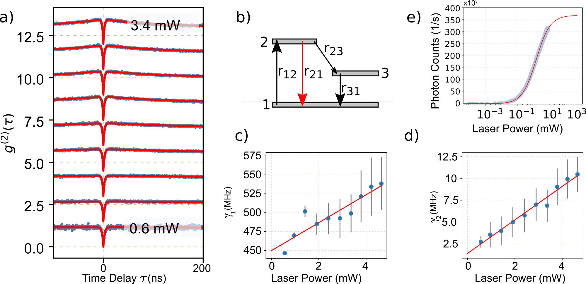
Figure 7.7: Optically pumped single photon emitter. a) BG corrected auto-correlations of the pl emitter as a function of the laser power. b) The suggested rate model for the pl emitters. c) and d) (left) and (right) rate parameters, respectively, extracted from a) are plotted as a function of the laser power. f) Photon counts of the pl emitter as a function of the laser power. See text for details.
Optically pumped single photon emitter
To investigate the p-i-n-device further, the same area is scanned with 730 nm laser illumination at zero applied bias. Remarkably, the el emitter stays dark in the laser illuminated scan. Instead, other emitters which are spatially and spectrally different to the el-emitter can be found.
In Figure 7.5 d a typical pl spectrum taken from the emitter, which is indicated by the dashed black circle in Figure 7.5 b is shown, and it becomes evident that the found pl-emitters are spectrally different when compared to the el-emitter shown in Figure 7.5 c.
Next the photon statistics of the pl-emitter is investigated. A typical laser power dependent dataset is plotted in Figure 7.7 a. Not only a clear photon antibunching of the pl-detected curves is observed. In addition a bunched feature occurs. The bunching shoulders are strong indicates for a metastable shelving state and can lead to spin-dependent photon emission. Such a observation is commonly found for single emitters in solids like diamond (Gaebel et al., 2004; Lee et al., 2013) and SiC (Fuchs et al., 2015; Widmann et al., 2015). To build up a similar rate model as for the el emitter, three-level model is used to describe the function (see Figure 7.7 b) (Aharonovich et al., 2010; Kurtsiefer et al., 2000):
where , and . Comparable to the two-level model, is depending on the optical excitation power , hence and can be rewritten as:
As shown in Figure 7.7 c), allows to determine , , and µs.
The presented rate-model can also be used to fit the saturation behavior plotted in Figure 7.7 e. The saturated count-rate was determined to 360 kcps.
Next, the polarization of both pl and el-emitter are investigated.
Photon Polarization Properties
In Figure 7.8 a and b the polarization patterns of the pl and el-emitter are shown, respectively. Clearly, most of both emitters types do exhibit very well linear polarized light emission. Only the pl-emitter plotted in green has non-ideal polarized dipole emission, which can be attributed to inhomogeneous background emission, leading to imperfect back ground correction.
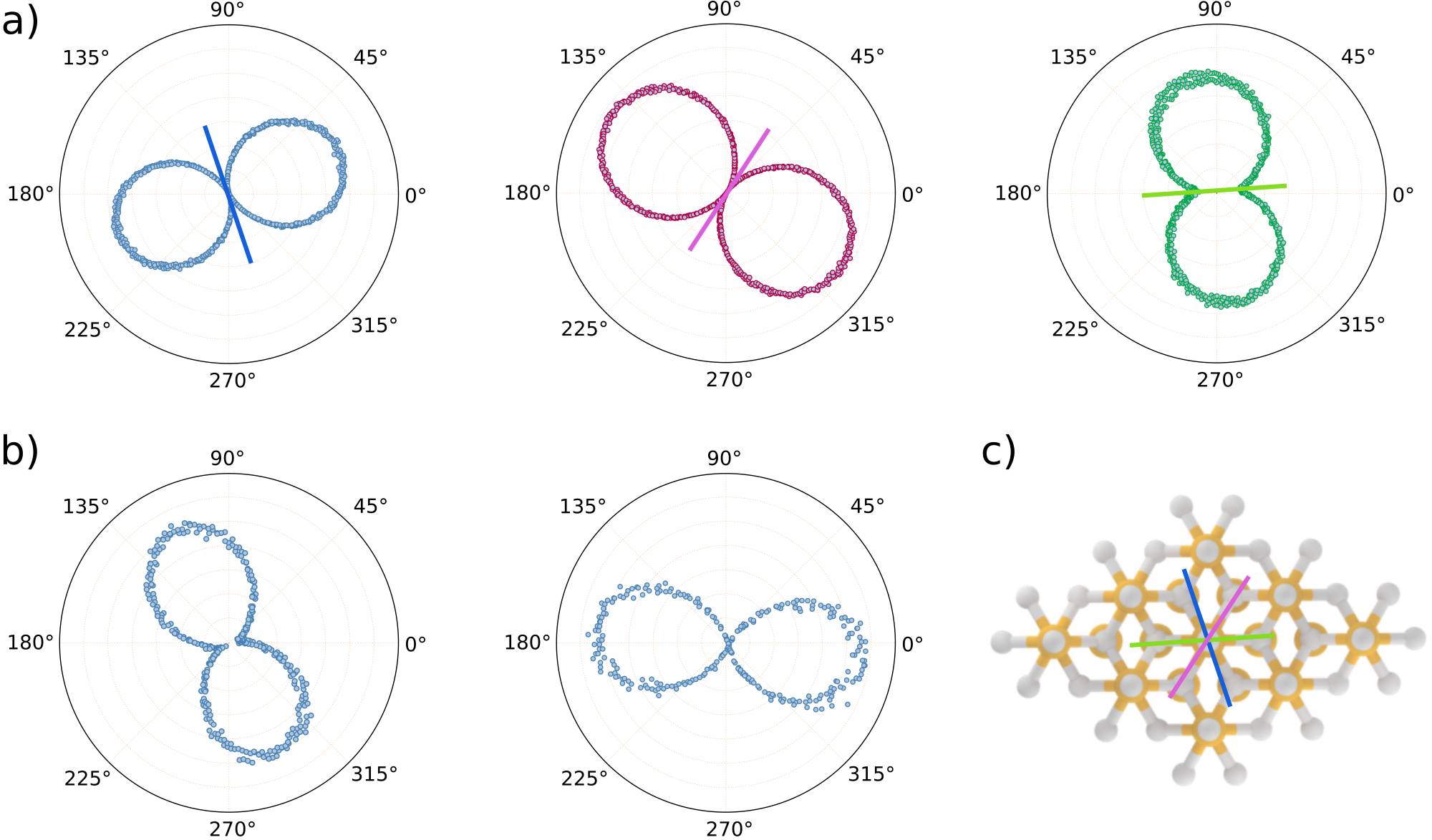
Figure 7.8: Photon polarization. of a) three pl emitters and b) two el emitters in the irradiated p-i-n device. c) Color coded dipole axes of the observed pl emitters with respect to the hexagonal lattice.
Three different dipolar emission pattern are found for 25 individually tested pl-emitters. They are found to be identical in excitation and absorption. When comparing to the basal plane crystal axes of 4H-SiC, their dipole axes are aligned to the three-fold symmetry as shown in Figure 7.8 c. Next, the polarization patterns for the el-emitters are presented in Figure 7.8 b. Here, ten different emitters have been tested for polarization but only two types of emitters with distinct dipole axes were found. They also match two axes of the basal plane.
In accordance with the experimental results, which tells that the pl and el-emitters are different in their spectral properties and do not coincide spatially, it can be concluded, that the emitters probably don’t have the same origin. However, it shall not be ruled out, that these defect have the same roots. Such behavior was found for isolated atomic scale defect in ZnO, where different excitation and decay pathways exist for el and pl (Choi et al., 2015). Recently, a variety of new color centers have been found on the SiC surface. Most of them were created without ion implantation or electron irradiation (Abe et al., 2018; Castelletto et al., 2014; A. Lohrmann et al., 2016; Sato et al., 2018). Here the samples were oxidized and are associated to defects in SiC at the SiC/SiO interface. These emitters also show photon polarization pattern, matching the three fold symmetry of the basal plane of 4H-SiC (Abe et al., 2018; A. Lohrmann et al., 2016). In consideration that the pl and el emitters presented in this chapter exhibit the same optical polarization dependence, one may tend to relate the found defects on the oxide interface at the SiC surface.
To get a deeper insight, whether the new type of emitters in this chapter were induced by electron irradiation, a non-irradiated reference sample with the same p-i-n diodes was investigated under optical illumination. The resulting confocal scan is presented in Figure 7.5 e with a representative spectra shown in Figure 7.5 f. The found pl spectra are shifted to the red spectral range. The observed spectrum is clearly different compared to the el and pl-emitters found in the irradiated sample and don’t match to the emitter recently reported (Abe et al., 2018; Castelletto et al., 2014; A. Lohrmann et al., 2016; Sato et al., 2018). In consequence these type of emitters are likely caused or induced by electron irradiation.
Conclusion and Outlook
In conclusion, three hitherto unknown color centers in non-irradiated and electron irradiated SiC lateral p-i-n diodes have been found and investigated. One species was noticed by charge carrier injection into the diodes intrinsic layer. The other two species were witnessed only by optical excitation in both type of samples. Despite the fact that the origin of all these emitters are not known yet, the oxide surface can be accounted for origin of the pl-emitters. Both the el and pl-emitters exhibit clear signatures of non-classical light emission. Their spectral emissions were found within the visible to the near infrared range. Both emitter types in the irradiated pin diodes show very well linearly polarized light emission. The dipole polarization axes match the hexagonal basal plane very well. As the origin was not revealed during this study, further work at low temperature will become necessary.
This chapter showed that SiC has the potential for a further fusion into modern electronic devices. It also showed the promising properties of SiC as a new material platform for various quantum applications in both quantum meterology and qip.