Doctoral Dissertation
Charge State Control
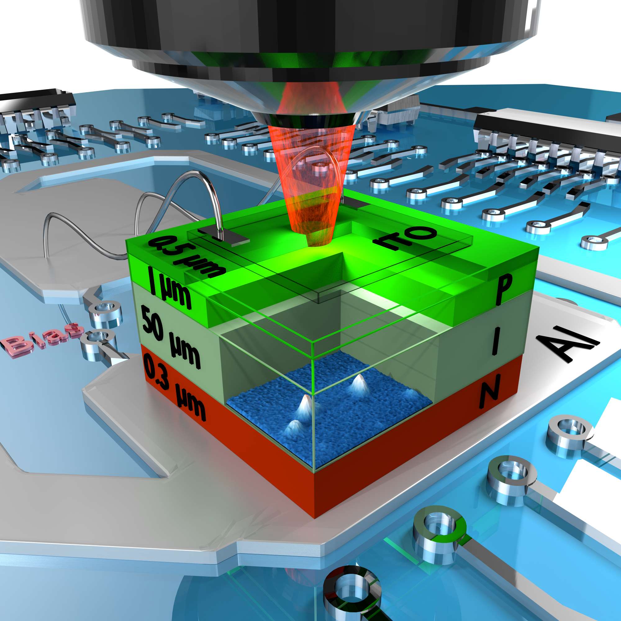
Figure 5.1: A SiC pin diode.
The results presented in the following chapter were partially achieved by an international collaboration with the following institutes:
- Department Chemistry and Physics of Materials, University of Salzburg, Austria
- Hungarian Academy of Sciences, Wigner Research Centre for Physics, Budapest, Hungary
- Laboratory of Nanooptics and Plasmonics Moscow Institute of Physics and Technology, Moscow, Russia
and shall become part of the publication:
M. Widmann, M. Niethammer, R. Nagy, C. Bonato, N. Morioka, S. Lasse, T. Rendler, R. Karhu, J. U. Hassan, N. T. Son, I. G. Ivanov, T. Ohshima, M. Bockstedte, A. Gali, D. Fedyanin, S.-Y. Lee and J. Wrachtrup, to be submitted.
Introduction
Defects in solids occur in multiple charged states, featuring distinct spin and optical properties. When a desired charge state cannot be established, often instability in the fluorescent emission hinders efficient optical detection (Bradac et al., 2010) and significant inhomogeneous broadening typically appears as well (Siyushev et al., 2013). For certain applications, it is also important to have control over the charge state of a spin-active color center. For example, the charge state control can open the way for selecting the properties which are relevant for the specific task. (Szász et al., 2015; Wolfowicz et al., 2017). As mentioned above, the negatively charged NV possesses an electronic spin (Grotz et al., 2012; Siyushev et al., 2013), but fast charge state conversion limits the efficiency of e.g. using it as a spin probe for sensing applications.
However, it can also be useful to temporarily switch the NV center to the spin-less charge state, and thus one can isolate the quantum states encoded on nuclear spin quantum memories by removing the spin-spin interaction to the NV center (Pfender et al., 2017; Saeedi et al., 2013). Another beautiful example is the charge state stabilization of the negatively charged NV state in diamond to keep the narrow optical transition necessary for efficient spin-photon interface (Hensen et al., 2015; Yang et al., 2016). Because different charge states are competing under optical excitation, the dynamics of charge state conversion should also be understood to realize efficient quantum control.
A convenient and potentially deterministic way to access any available charge states is to use an electrical device to tune the Fermi level relative to the defect energy levels. As already mentioned: in large bandgap materials such as diamond, this is not trivial due to difficulties associated with doping. SiC can provide a solution to these issues. The following presented explanation of the charge state switching was (partially) under controversial debate during time of writing. The improved version may be found in the above mentioned publication.
PIN-Diode Fabrication
In Figure 5.2a the structure of the p-i-n diode is shown. The p-i-n stack was grown by cvd on a on a 4-degree off-cut 4H-SiC substrate, whose fabrication process is explained in the following.

Figure 5.2: Device geometry. a) Schematic of the used pin structure and the respective doping layers (for doping concentration see text.). Metallic base plate is made of aluminum (grey). b) Top view of the device under forward applied bias showing a mixture of blueish and greenish light emission, presumably from D1 center (Pinheiro et al., 2004; Rauls et al., 2005). Photograph taken with Panasonic FZ1000 camera with exposure time of 5 s.
The substrate a n-type doped 4H-SiC with concentration of 9×10¹⁸ cm⁻³ and resistance of 0.017 Ω cm⁻¹ and sizes 509 μm in thickness. Next the n-type layer was grown with 9×10¹⁸ cm⁻³ with a subsequently grown intrinsic region, which was found to be slightly p-type with a concentration of 1×10¹³ cm⁻³. Al-doped p-type layer with a doping concentration of 1×10¹⁸ cm⁻³ grown to obtain p-i-n stack. An Al concentration of 1×10¹⁹ cm⁻³ was grown on the top with a thickness of 500 nm to realize a p-type contact with a thickness of 500 nm. To enable both, electrical and optical access to the device a conductive and transparent ito-layer, with a thickness of 200 nm was deposited on the last -type layer. Al electrodes were deposited on small regions (see Figure 5.2b on top of the ito-layer which were wire bonded to a separated base plate (not shown) to apply a bias to the device.
With the aim to create silicon vacancy the device was electron irradiated with 2 MeV electrons. As the penetration depth of the 2 MeV electrons is about 2 mm, a homogeneous distribution over the whole sample thickness can be ensured.
One important aspect is found in the fact, that the intrinsic layer was unintentionally slightly p doped due to residual Al/B originating from previous growth which was not compensated by nitrogen. Hence, the resulting doping level of the first μm above the gradually changes to slightly p-type. In essence the intrinsic region is not a real intrinsic 4H-SiC but low doped p-type 4H-SiC with unknown exact doping, but estimated to 1×10¹³ cm⁻³. That will have consequences on the band structure and the spatial location of the which experience a switching behavior (see upcoming sections).
The p-i-n device was first tested as a bare device under forward applied bias as shown in Figure 5.2b. The injected current is provoking light emission, commonly known as electroluminesence. A historical side-mark, the first light emitting diode (LED) was made of silicon carbide in 1907 (Round, 1907), and light emission has been reported multiple times (Szigeti, 1954; Vasenkov et al., 1969).
Energy-Band Diagram Simulation
In Figure 5.3c) and d) the simulated band diagram with =1×10¹³ cm³ and =1×10¹⁴ cm³ is shown, respectively.

Figure 5.3: Energy band diagram simulation. a) For doping concentration of 1×10¹³ cm⁻³ and b) for 1×10¹⁴ cm⁻³. Left panel: negative bias. Middle: zero bias. Right: positive bias. In green: the quasi Fermi level for electrons. The charge state transition levels for are indicated with black () and purple () lines.
The stronger intrinsic region is p-type doped the band bending moves towards the n-type doped area. As above mentioned that will impact the region where charge state switching of can be observed. The ito layer is excluded from simulation. It is known that ito forms a Schottky contact on p-type SiC (Hwang et al., 1996). Based on calculation by D. Fedyanin et al. the ito does not change the overall band-structure, and hence for the charge state switching this layer does not play an important role.
Results
Irradiation Dose Dependency

Figure 5.4: Irradiation dose dependence. a) Schematic of the used pin structure and the experimental configuration. Metallic base plate is aluminum, red layer indicates the highly n-type (1×10¹⁸ cm⁻²) layer. Grey layer represents the intrinsic region which is slightly p-doped (1×10¹³ cm⁻²), green as the highly p-doped layer 1×10¹⁸ cm⁻² and the transparent layer is ito. b) Defect density of photo-active V_{\text{Si}}$${}^{(-)} measured at the i-n interface and plotted as a function of the irradiation dose. Reference data set plotted in grey/blue from cvd grown 4H-SiC. The emitter density of the lower irradiation doses are determined at the interface of the i-n-layer. c) Room temperature confocal scans obtained at 1.5 mW at 730 nm, and used in b) for defect density determination.
To investigate the impact on emitter density of the electron irradiation dose for the fabricated diodes, two-dimensional confocal scans of the devices is performed for various irradiated pin-diode at zero applied bias as shown in Figure 5.4.
Compared to the samples with Si-SiC the pin-diode sample exhibit a lower concentration of optically active V_{\text{Si}}$${}^{(-)}. As the sample is slightly p-type in the intrinsic region the might be in another charge state.
Defect Density Depth Dependence
With the aim to accurately determine the depth of the investigated emitter, it mandatory to know the psf of the microscope.

Figure 5.5: Geometrical ray optics considerations. for aberrations induced by refraction at the oil-SiC interface. Graph created by Naoya Morioka.
In high refractive-index materials, such as silicon carbide or diamond, serious aberrations are introduced. Consequently the real focus of the objective is shifted deeper into the medium (see Figure 5.5). In addition, the excitation laser light also experiences aberrations. Therefore, both of the psf for emitters and the excitation depth of the laser need to be considered. (Macquarrie et al., 2013). In the following a model is developed (by Naoya Morioka) to correct for these aberrations. The intensity distribution of the laser is of the form , where is calculated with and being the full-width-half-maximum. The beam is focused, when sent through an objective with a back focal plane and na. The laser enters the crystal with an incident angle at the radial position . The refraction which occurs at the oil-crystal interface is calculated with Snell’s law. According to Abbe’s condition the radial distance is calculated by:
(5.1)
where the maximum incident angle is defined by . Using the intensity distribution and Equation 5.1 the intensity distribution can be rewritten as a function of . The light is focused at , when no crystal is present. The differential power at can be expressed with:
(5.2)
The Fresnel transmission coefficient is given by:
(5.3)
The depth of the psf inside the SiC medium can be related to the depth in the immersion oil as
(5.4)
Where, and are the refractive indexes of the 4H-SiC and the used immersion oil, respectively. The average value for can then be expressed by combining Equation 5.3, Equation 5.3 and Equation 5.2:
With 8.1 mm, and 2.5 mm the average value is calculated to 1.8 . The obtained correction factor is used to correct for all measured emitter depths inside the pin-diode, as shown in Figure 5.6.
With the aim to investigate the impact of the doping level for optically active V_{\text{Si}}$${}^{(-)}, a two-dimensional confocal scan of the lowest irradiated device was performed across the growth direction (-axis). The spatial distribution along -direction is illustrated in Figure 5.6. Isolated emitters can be found across the whole intrinsic layer by optical excitation with 1.7 eV (730 nm). These isolated emitters are in the negatively-charged state (V_{\text{Si}}$${}^{(-)}) which was confirmed by odmr measurements (see Figure 5.9 b).

Figure 5.6: Depth distribution of negatively charged silicon vacancies. a) Schematic of the p-i-n structure. b) Room temperature confocal scan through the intrinsic layer.
No V_{\text{Si}}$${}^{(-)} pl emission is present both in the n-type layer and in the substrate. It is known that the V_{\text{Si}}$${}^{(-)} center can be found in n-type SiC such as in semi-insulating SiC while high p-type doping ([Al]510-410 cm) does not allow observation of V_{\text{Si}}$${}^{(-)} (Son et al., 2007).
However, the V_{\text{Si}}$${}^{(-)} center has recently been found in slightly less p-doped SiC ([Al]510 cm) (Bracher et al., 2016) which matches the observation of optically active in a low p-doped regime of this work. This is likely due to the charge state transition via optical ionization, and will be explained later in Section 5.4.4. First the V_{\text{Si}}$${}^{(-)} distribution near the i-n interface is investigated. Here, the band-bending is expected to have a drastic impact on the charge state transition. As explained later in Section 5.4.4, band bending stabilizes different charge states at various depths and the interplay with optical ionization and recombination causes complex charge state transition dynamics.
Charge State Switching
To further investigate charge dynamics a bias is applied to the junctions and multiple are investigated in terms of the switching bias and the vertical location. While V_{\text{Si}}$${}^{(-)} in the intrinsic layer do not show significant changes in their concentration, V_{\text{Si}}$${}^{(-)} near the i-n interface responds to the applied bias drastically.

Figure 5.7: Charge state switching. Confocal scans at the same spatial location with various applied biases obtained with 1.5 mW optical excitation at 1.7 eV (730 nm) illustrating the charge state switching behavior of near the i-n interface.
Figure 5.7 shows confocal raster scans of the same area under reverse (left), zero (center) and forward (right) applied bias near the i-n interface where the density of V_{\text{Si}}$${}^{(-)} emitters is increased (=50 μm). At reverse bias, several emitters are turned on, while the forward bias turns off the emitters which are bright at the zero bias. One can attribute this to switching of the charge state of V_{\text{Si}}$${}^{(-)} to other dark charge states due the non-equilibrium induced by the applied bias.
As introduced in Section annealing, the silicon vacancy can exist in four charge states, namely in , , and as calculated with dft (Hornos et al., 2011), and its charge state is defined by the position of the Fermi-level .

Figure 5.8: Charge states of the silicon vacancy in 4H-SiC. Silicon vacancy charge states, exemplarily for the k-site.
When only , , charge states are considered, the probability to find in the single negatively charged state can be expressed using Fermi-Dirac statistics:
Here are the respective degeneracy factors for the charge states ,, . The energy levels for the charge state transitions are defined as . As it becomes evident from the equation above the probability depends on and . The following limiting cases can be distinguished:
To account for the additional charge state the equation above is modified to:
Clearly this modification does not affect the population of V_{\text{Si}}$${}^{(-)}, and the first equation is a good approximation.
In addition, the newly switched-on emitters at an applied reverse bias are located at a slightly further distance from the n-layer (see Figure 5.7 bottom panel). To check if the switching depends on the position, the pl intensity of each bright emitter is monitored while sweeping the bias voltage. Two selected results are shown in Figure 5.9b. The pl intensity is completely turned off at the forward bias, while it is bright at the reverse bias. The sharp increase in the pl intensity, which is found at the bias value inducing the switching will be discussed later in Section 5.4.4.

Figure 5.9: Vertical distribution of switchable silicon vacancies. a) pl intensity of two selected located at near i-n interface as a function of the applied bias, illustrating the switching at different applied bias. b) Top: pl intensity of another selected . Bottom: Chirped odmr measurement showing the spin signal of V2. c) Simulation of the spatial dependence of the charge state distribution at zero bias. Simulation performed by D. Fedyanin. d) Switching bias as a function of vertical positions of . The switching bias is extracted from a), and the vertical position of the location is taken from Gaussian fits. For a) and d), excitation laser at 5.5 mW, 1.88 eV (660 nm) was used.
From Figure 5.9a it is evident, that the shown two emitters exhibit the switching of the V_{\text{Si}}$${}^{(-)} pl at different voltages, namely the switching bias. In Figure 5.9b another selected emitter is shown, on which a chirped odmr-measurement1 was performed (indicating ) existence. It shows no spin signal when the emitter is not V_{\text{Si}}$${}^{-}. To check if there exists a relation between the switching bias (the voltage at PL) and the vertical position of each emitter, several confocal -scans around each emitter were performed. The -position was obtained by fitting the depth distribution of the pl intensity with using a Gaussian function. This process was repeated on several emitters. Then the relation between the position and the switching bias of each emitter was extracted, as illustrated in Figure 5.9d. The plot shows that a stronger reverse bias is necessary to switch V_{\text{Si}}$${}^{(-)} emitters on for emitters further from the i-n-interface. In other words, the reverse bias expands the region where V_{\text{Si}}$${}^{(-)} emitters are bright into the i-layer.
This experimental finding can be compared to theory by using , obtained by the device simulation from Section 5.3, and the Fermi-Dirac equation above. The region where stable V_{\text{Si}}$${}^{(-)} are expected is obtained. The simulation result is plotted in Figure 5.9c and the corresponding measurement data in Figure 5.9d.
The simulation in Figure 5.9c match qualitatively the measured spatial dependence in Figure 5.9d. A quantitative match will require more detailed investigation into several properties of the device. One critical parameter is the unknown doping of the intrinsic region. In addition to this, the profile of the doping transition from n-type to p-type is not precisely known. Additionally, hitherto unknown resistances at, for instance, the metal-semiconductor interfaces also lead to a linear scaling of the real bias voltage.
By considering only the Fermi level with respect to the energy level of each defect located near the i-n interface, a is expected to be the neutral charge state V_{\text{Si}}$${}^{(0)} in the slightly p-doped intrinsic layer. Also the increase of the Fermi level with respect to the valence band will increase the chances for a to capture more electrons. Therefore, one may expect a monotonic increase in the V_{\text{Si}}$${}^{(-)} concentration while approaching to the n-layer. The double negatively charged state V_{\text{Si}}$${}^{(2-)}, is dark in the tested spectral range, the concentration of luminescent spots should become lower at the positions very close to the n-layer. In contrast to this simple expectation, the experimental results in Figure 5.7 and Figure 5.9 suggest that the charge-state dynamics of may be complicated under optical illumination. One key factor that can impact on the charge state is optical excitation, since it can cause ionization of the defects, which then capture or emit electrons.
Charge States and Ionization
To test how optical excitation is related with the charge state formation, one single vsi defect is selected and its pl intensity is monitored as a function of the applied bias while the optical excitation energy (wavelength) is varied. The results are shown in Figure 5.10. In Figure 5.10a, the integrated pl intensity in the range from 900–1050 nm from a single near the i-n interface is plotted as a function of the applied bias, for optical excitation of 1.88 eV (660 nm).

Figure 5.10: Bias and wavelength dependent PL intensities. as a function of applied bias under different excitation energy of a) 1.88 eV (660 nm) b) 1.7 eV (730 nm), and c) 1.61 eV (765.5 nm). d) Charge state transition levels of silicon vacancy (left panel), and carbon vacancy (Coutinho et al., 2017) (right panel) at various Fermi-levels conditions distinguished by encircled numbers. See text for details.
For the tested emitter, switching is observed at around zero bias, with the sharp increase in the pl intensity as shown in Figure 5.10a. The experiment was repeated for different excitation energies as in Figure 5.10b and c. When the optical excitation energy is larger than 1.60 eV (773 nm) a similar behavior (see Figure 5.10 a,b,c) is observed.
To explain that behavior, one has to consider another prominent defect in SiC, namely the carbon vacancy . The concentration is in the range of 5×10¹²–10×10¹³ cm⁻³, measured for similar samples by dlts in Linköping. Since this concentration corresponds to the average distance between neighbor of about 300 nm ( diffusion length is about 1 μm) (Bathen et al., 2018), there is a large probability for a to be located near the , affecting the charge state of the nearby .
The defect can exist in either single donor (|0) or double donor (2|) levels deep in band gap (Bockstedte et al., 2010; Hornos et al., 2011; Trinh et al., 2013; Umeda et al., 2004; Zywietz et al., 1999). In addition, it possess two negative-U double acceptor levels near the conduction band edge (Kawahara et al., 2013, 2014; N. T. Son et al., 2012; Trinh et al., 2013) and is often referred to -center in literature, when is in these charge states.
At positive bias (see top panel in Figure 5.10a) and b, the is in the () charge state, determined by , and optical ionization can convert V_{\text{Si}}$${}^{(3-)} to V_{\text{Si}}$${}^{(2-)} and no V2 pl is visible. Considering , optical excitation with photon energy of 1.6–1.7 eV can promote electrons from the to the conduction band, i.e. V_{\text{C}}$${}^{(+)} \rightarrow$$V_{\text{C}}$${}^{(2+)}+e or V_{\text{C}}$${}^{(0)} \rightarrow$$V_{\text{C}}$${}^{(+)}+e (Bockstedte et al., 2010).
At zero bias, is located mid-gap (Figure 5.10d) middle panel). The is in the () charge state, which gives rise to characteristic V2 pl emission. The increased pl-intensity may be explained by considering the . When is found in ()-state, optical ionization to the conduction band is possible with photon energy > 1.61 eV (730 nm). The photon energy is very close to the optical ionization threshold of V_{\text{C}}$${}^{(+)} \rightarrow$$V_{\text{C}}$${}^{(2+)}+e or V_{\text{C}}$${}^{(0)} \rightarrow$$V_{\text{C}}$${}^{(+)}+e. Another plausible explanation can be found in the combined dynamic processes of quenching of V_{\text{Si}}$${}^{(-)} by electron capture V_{\text{Si}}$${}^{(0)}+e{}^{-} \rightarrow$$V_{\text{Si}}$${}^{(-)} triggered by V_{\text{C}}$${}^{(+)} \rightarrow$$V_{\text{C}}$${}^{(2+)}+e or V_{\text{C}}$${}^{(0)} \rightarrow$$V_{\text{C}}$${}^{(+)}+e and optical ionization V_{\text{Si}}$${}^{(2-)} \rightarrow$$V_{\text{Si}}$${}^{(-)}+e. This effectively “re-initializes” V_{\text{Si}}$${}^{(-)} and as a result yields an enhanced pl-intensity. An optically excited V_{\text{Si}}$${}^{(-)} can either radiatively decay by emitting a photon (lifetime 8 ns) or decay through a dark metastable state (lifetime around 100 ns). For V_{\text{Si}}$${}^{(-)}, decay into the metastable state is very frequent, with a time constant comparable to radiative decay to the ground state (16 ns), resulting in reduced photon emission rates. However, re-initialization, as outlined above, could take the population out of the dark long-lived metastable state, increasing the optical excitation and emission rates. Because excess electrons can be provided by V_{\text{C}}$${}^{(+)} \rightarrow$$V_{\text{C}}$${}^{(2+)}+e or V_{\text{C}}$${}^{(0)} \rightarrow$$V_{\text{C}}$${}^{(+)}+e, this process is enhanced at higher laser power, as shown in Figure 5.11c).
At negative bias (see Figure 5.10 bottom panel) is in the () charge state, and is in the () charge state. In this case no optical ionization process of V_{\text{C}}$${}^{2+} is possible anymore, because < 1.69 eV, which is smaller than the energy difference of cb-V_{\text{C}}$$(2+|+). However, V_{\text{Si}}$${}^{0} can be optically pumped from vb to V_{\text{Si}}$${}^{-} and gives rise to V2 pl emission.

Figure 5.11: Bias and wavelength dependent PL intensity 2. Integrated pl intensities as a function of the applied bias under different excitation energy of a) 1.60 eV (773 nm) and b) 1.58 eV (785 nm). c) Optical saturation curves measured with 1.88 eV at V bias (red curve) and zero bias (blue curve). d) Charge states of silicon vacancy (left panel) carbon vacancy (right panel) at various Fermi-levels conditions indicated by encircled numbers. See text for details.
To substantiate this process involving ionization processes of the , the experiment was repeated for < 1.61 eV as shown in Figure 5.11a and b. With < 1.60 eV no sharp peak in pl intensity is observed at the switching bias (Figure 5.10 d) and ,e)). The previously possible photo-ionization processes of is by energy consideration not possible any more.
To summarize the experimental findings discussed above:
- V_{\text{Si}}$${}^{(-)} emitters appear in the i-layer (slightly p-doped layer).
- Local minimum of the V_{\text{Si}}$${}^{(-)} emitter concentration can be found near the i-n interface.
- V_{\text{Si}}$${}^{(-)} emitter concentration increases further close to the i-n interface.
- V_{\text{Si}}$${}^{(-)} emitter can be switched by applying bias.
- An extension (contraction) of the layer where V_{\text{Si}}$${}^{(-)} emitters can be observed near the i-n interface into the i-layer is detected by applying reverse (forward) bias.
- A sharp peak in the pl intensity at switching bias is observed only when the applied optical excitation energy is larger than 1.61 eV.
In the following, underlying mechanisms responsible for the above observations will be discussed.
Only V_{\text{Si}}$${}^{(-)} is known to exhibit pl in the spectral region 900–1050 nm and hence is observed as a bright state under the experimental conditions. In the intrinsic layer, is below the transition level (), due to slight p-type doping. Hence V_{\text{Si}}$${}^{(0)} is expected to be stable without optical excitation. However, V_{\text{Si}}$${}^{(0)} may be converted into V_{\text{Si}}$${}^{(-)} by optical excitation of electrons from the valence band into the defect levels by photon energies above a conversion threshold E.
From the absorption spectrum of V_{\text{Si}}$${}^{(0)}, calculated by M. Bockstedte et al. using the crpa approach, the optical excitation threshold 0.8 nm (1550 nm) for the conversion of V_{\text{Si}}$${}^{(0)} into V_{\text{Si}}$${}^{(-)} was obtained. Photon energy of 0.8 eV will move electrons being trapped in the () state of , located at 0.56 eV, for (h) and 0.71 eV, for (k) below the conduction band minimum, to the conduction band. These free electrons can be captured by V_{\text{Si}}$${}^{(0)} and turn it to V_{\text{Si}}$${}^{(-)} (N. T. Son et al., 2012; Trinh et al., 2013).
Optical excitation with photon energy of 1.6–1.7 eV will be able to promote electrons from the to the conduction band. A part of these electrons can be captured to V_{\text{C}}$${}^{(2-)}, so even in slight p-type intrinsic layer at room temperature, there can always be electrons in the V_{\text{C}}$${}^{(2-)} trap level.
Because a 1.7 eV (730 nm) laser is used for the data in Figure 5.6 and Figure 5.7, the V_{\text{Si}}$${}^{(-)} can be observed across the whole i-layer. Close to the i-n junction, the steep band-bending makes cross various charge state transition levels. Hence defects are expected in different charge states depending on its depth along the z-axis. However, charge state transitions in this regime cannot be easily understood by considering only the Fermi-level with respect to each transition level. For example, highly charged states, e.g. V_{\text{Si}}$${}^{(2-)} and V_{\text{Si}}$${}^{(3-)}, which are likely to be stabilized when E_F$$\mathrm{>} 2.47 eV and 2.74 eV, can also be ionized by lower-energy optical excitation. Furthermore, additional screening effects due to other impurities may occur, and can act as a shield for the silicon mono vacancy. This can result in a shifted bias necessary to switch the .
Note that V_{\text{Si}}$${}^{(-)} \rightarrow$$V_{\text{Si}}$${}^{(0)}+e is not expected assuming only single photon absorption process in the given experimental conditions. The absorption process requires photon energy E{}_{L}$$\mathrm{>} 2.03 eV (612 nm), while the highest energy used in this study is only 1.8 eV. In addition, optical ionizations of other nearby defects also have to be considered. As discussed above is the most abundant intrinsic defect in SiC. Depending on the and the optical excitation energy, ionization of various charge states can occur. For instance, if 1.67 eV\mathrm{<}$$E_F$$-E_V\mathrm{<}1.84 eV, can be found in the V_{\text{C}}$${}^{(+)} state, which can be optically ionized to V_{\text{C}}$${}^{(2+)} only by an optical excitation energy at or larger than 1.69 eV (Bockstedte et al., 2010).
A summary table with the expected charge states for both and , considering only , and optical ionization is provided in the appendix. It shows the complexity of the charge state conversion mechanism near the i-n interface. In addition, the excess charge carriers are released by the optical ionization, which can be recombined at other defects as well. As above mentioned, in the discussed sample, the concentration is in the range of 5×10¹² cm⁻³ to 10×10¹³ cm⁻³, measured by dlts. Since this concentration corresponds to the average distance between of 300 nm, there is a good chance for a to be located near the , affecting the charge state of the nearby . For example, a released electron via V_{\text{C}}$${}^{(+)} \rightarrow$$V_{\text{C}}$${}^{(2+)}+e by E{}_{L}$$\mathrm{>}1.69 eV may be captured by a nearby which result in e.g. V_{\text{Si}}$${}^{(-)} +e{}^{-}\rightarrow$$V_{\text{Si}}$${}^{(2-)}. This complexity is raised further by the non-equilibrium induced by the applied bias. Hence, it is not trivial to understand every detail presented in this chapter.
Conclusion
In this chapter the charge state switching of a single silicon vacancy near the i-n interface in an opto-electronic 4H-SiC pin diode was investigated. It was found that the charge state switching is determined by the Fermi level and by optical ionization. The charge state of the silicon vacancy is controlled by applying bias and changing the optical excitation energy and intensities.
It was shown that the charge state of the bright silicon vacancy is also determined by optical ionization of a nearby located carbon vacancy. The lowest lying charge state transition level for the donor type carbon vacancy is higher in energy as the acceptor type silicon vacancy. When the carbon vacancy is in the () charge state, an electron can be optically ionized and can be recaptured by nearby silicon vacancy. This hypothesis is supported by wavelength dependent photo ionization measurements, which showed that optical ionization is only possible if the photon energy is larger than 1.69 eV. Further work is required to understand precisely the complex interplay of the involved competing processes, such as emission and recombination of excess charge carriers at both and . Combining the method used in this chapter with other junction spectroscopic methods such as dlts may allow to gain more information. In conclusion, this chapter examined the possible charge state conversion mechanisms for the silicon vacancy defects in SiC, an important prerequisite for improved control over their quantum properties and their application to quantum technology.
Footnotes
-
Chirped odmr means, that all spin transitions are driven by quickly sweeping rf over 40-90 MHz. ↩