Doctoral Dissertation
Basics
Introduction
The following chapter is dedicated to providing an overview of the unique physical properties of SiC as a material.
That includes a brief overview of state-of-the-art growth methods of SiC in Section 1.2.2, as well as doping possibilities presented in Section 1.2.2.4, which is important for the electronic (quantum) devices presented in Chapter 5 and Chapter 7. Section 1.3 is a review of intrinsic defects with a main focus on the optical and spin properties of the silicon vacancy center in silicon carbide. The experimental apparatus is presented in Section 1.6.
Properties of Silicon Carbide
Silicon carbide is composed of silicon (Si) and carbon (C) atoms. It is the only IV-IV semi-conducting material known to mankind. It can be understood as the intermittent material between diamond and silicon, sharing advantages of both materials (see Table 1.1). For example, it has a high thermal conductivity, high breakdown voltage and a wide band gap. These properties make SiC to one of the most promising materials for high temperature and high power electronic, electromechanical as well as optoelectronic devices.
SiC has typical band gap of around 3 eV, and owes excellent possibilities for n-type and p-type doping (Straubinger et al., 2002). Both, the large band gap and doping possibilities of SiC combined with a high thermal conductivity is also the reason why SiC became an important material for high power devices. More electrical energy can be sent through a same sized chip when compared to silicon. Diamond with a larger band gap of around 5.5 eV would suit in that respect even better, but suffers from complicated n-type doping.
Table 1.1: Fundamental properties of diamond, silicon and silicon carbide.
| diamond | SiC | silicon | |
|---|---|---|---|
| band gap | 5.5 (Wort & Balmer, 2008) | 2.3–3.3 (Madelung et al., 2002) | 2.3 (Madelung et al., 2002) |
| thermal conductivity (W/cmK) | 10–25 (Slack, 1964) | 4.9 (Slack, 1964) | 1.12 (Slack, 1964) |
| breakdown field (MV/cm) | 10 (Wort & Balmer, 2008) | 3 (Madelung et al., 2002) | 0.3 (Wort & Balmer, 2008) |
| hardness (Mohs) | 10 | 9.5 | 6.5 |
| dielectric constant (, ) | 6.52, 6.7 (Sze & Ng, 2006) | 11.7 (Seeger, 1988) |
Crystal Structure
Silicon carbide is a semiconductor with covalent bonds between Si and C.

Figure 1.1: Building blocks of SiC. a) Type 1, b) rotation by 180° results in type 2. Adopted from (v. Münch et al., 1976).
It is a hard material owing to the short bond length of 1.89 Å and this leads to its good mechanical, chemical and thermal properties. In the crystalline form, each carbon atom is bonded to four neighboring silicon atoms and vice versa, forming a tetrahedron. Two types of such tetrahedrons occur in SiC. Type 1 is obtained by a rotation of of a tetrahedron along the c-axis of the crystal. Type 2 is obtained by mirroring type 1 parallel to -axis (see Figure 1.1).
The c-axis is aligned normal to the Si-C layers. Carbon, or silicon atoms are hexagonal closed-packed (hcp) in each layer. The double-layers (Si-C layers) can be arranged in three different configurations, labeled as A,B,C. A distinct repetition of the double-layers along the -axis of the crystal form a certain polytype. The first classification of the polytypes is made based on their crystal symmetry, represented by capital letters (C=cubic, H=hexagonal, R=rhomboedric). The stacking sequence ABCABC of the double-layers form 3C-SiC, and has cubic symmetry. This type is also known as -SiC, and is the only cubic form of SiC. Hereby, the number before letter C denotes the number of bi-layers which are used. All hexagonal types start with the configuration of 2H-SiC. In consequence local cubic and hexagonal lattice sites of the second neighbors occur, denoted as and , respectively (see Figure 1.2 and Table 1.2). The hexagonal rate describes the relative proportion between cubic and hexagonal lattice sites along the c-axis, and can be calculated according to .

Figure 1.2: Polytypes of SiC. for the three most common polytypes 3C, 4H and 6H SiC. In 3C only cubic lattice exist, whereas for the hexagonal types mixtures of cubic and hexagonal are present. Adapted from (Stephen E. Saddow, 2004; v. Münch et al., 1976).
The polytype of a SiC-crystal can be determined via Raman scattering measurements. Because of the strong covalent bonding the Raman efficiency of SiC is high, which allows for fast and accurate polytype determination (Nakashima & Harima, 1997).
Table 1.2: SiC: Crystallographic Notations. Adapted from [@Hornos2008].
| Ramsdell | Jagodzinski | ABC | Hexagonality | Symmetry |
|---|---|---|---|---|
| 3C | kkk | ABC | 0% | T |
| 2H | hh | AB | 100% | C |
| 4H | khkh | ABAC | 50% | C |
| 6H | hkkhkk | ABCACB | 33% | C |
The large variation of the possible stacking-sequence is the reason for different SiC polytype formation; about 250 distinct types are known (Fisher & Barnes, 1990), each of them owing different physical properties, which affects optical and electronic properties. For example, each polytype has a different band-gap, thermal conductivity, refractive index, and different electron-mobility.
Industrially dominant polytypes are 4H, 6H and 3C-SiC. In particular 4H-SiC is used for high power applications because it offers (beside 2H-SiC) the highest band gap and has an isotropic electron mobility (Schaffer et al., 1994). In this work 4H-SiC polytype is used, because high purity crystals can be made fairly easy with a concentration of uncontrollable impurities less than cm⁻³.
Growth process
The growth of monocrystalline SiC with high quality has become a very well developed technology (Kordina et al., 1996; Lely, 1955; Tairov & Tsvetkov, 1978). The first artificially grown SiC was produce by Lely et al (Lely, 1955) in 1955, which essentially bases on a PVT method (see Figure 1.3 a).
Another commonly used crystal growth technique is cvd at high temperatures (Kordina et al., 1996) which is known as htcvd (see Figure 1.3b). Both techniques allow to grow large SiC single crystals, diameters of 15 cm are routinely achieved. PVT is known to be a well established, inexpensive and stable method. The advantage of cvd is the precise control of process parameters, in particular doping (Muller et al., 2006). A representative example for an industrially grown SiC sample is shown in Figure 1.4.

Figure 1.3: SiC growth processes. a) PVT-method. The SiC powder is sublimated and condenses on a SiC crystal (blue disk on top) HTCVD-method. A gas mixture is introduced into the chamber from top. The SiC substrate (blue disk at the bottom) is rotated. Adopted from (v. Münch et al., 1976).
PVT-method
The PVT method relies on the sublimation of a polycrystalline SiC source, which is typically in powder form. The schematic of the reactor is shown in Figure 1.3a. The heat for the sublimation is achieved by inductively heating a porous graphite crucible with copper coils. Hereby, the SiC source is placed in the hot zone of the growth chamber where the sublimation is taking place. The vapor phase of SiC is transported to the cooler zone of the growth chamber and condenses on a SiC substrate (Heydemann et al., 1996; Tairov & Tsvetkov, 1978).
HTCVD-method
htcvd is an expansion of the cvd technology simply at much higher growth temperature, which is typically larger than 1900 °C. A schematic of an htcvd-reactor is schematically shown in Figure 1.3b. A water-cooled quartz tube hosts a hot wall and a susceptor. The susceptor rotates with typical speeds of around 10 rpm. The hot wall is heated by induction coils. The thermal radiation from the wall heats the susceptor and the substrate. From the top of the reactor as carrier gases and as precursors are introduces. The gas is heated before hitting the substrate.
Both the PVT and the htcvd techniques allow the production of semi-insulating, n- or p-type crystals with high purity. Large SiC wafers with diameters up to 150 mm is state of the art in industrial SiC production.
Polytypes
Formation of a certain polytype is dependent on a large variety of growth parameters in the nucleation stage, such as seed polarity (Stein & Lanig, 1993), crystal growth temperature, supersaturation, vapor phase stoichiometry (Tairov & Tsvetkov, 1983), impurity levels, seed off-cut angle (Rost et al., 2006), and influence of the facet have been studied in regard to polytype control (Tupitsyn et al., 2007). The initial polytype formed at almost all growth temperature is 3C-SiC and acts hereby as precursor for the phase transformation to other polytypes.
Doping
Same to other semi-conductors, doping allows to tune the electric properties of SiC and the creation of complex electronic devices.
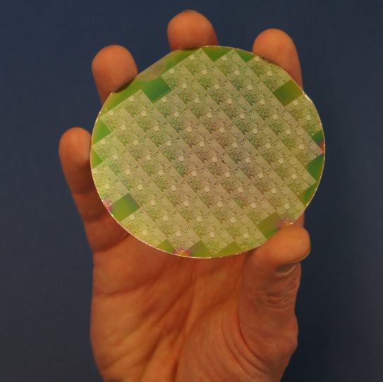
Figure 1.4: SiC wafer.
It is a well established process technology, a 4 inch wafer is shown in Figure 1.4. The structures on the wafer are electronic structure, such as field effect transistors, etc… Such structures require n and p type doping. For n-type doping in SiC nitrogen is a widely used dopant (Muller et al., 2006). To achieve p-type material the most dominant dopant is aluminum (Forsberg et al., 2003), but phosphorous and boron can be used as well. Aluminum has advantages compared to Boron, because aluminum forms shallower acceptor levels (Miyazawa et al., 2016). At the same time Al occupies the atomic silicon more likely than Boron. This makes Al more suitable for the production of heavily doped SiC layers with low resistances (Miyazawa et al., 2016).
In cvd, doping can be controlled by introducing additional vapors during growth, (eg. for n-type doping is used). P-type doping is achieved by introducing , , to the precursors. Hereby atoms substitute the silicon atoms. Doping can also be achieved by post-implantation of ion species into the crystal. Semi-insulating layers can be grown through in-situ vanadium doping during growth, using vanadium tetrachloride (VTC) in bubbler configuration (Negoro et al., 2004).
Defects and Color Centers
In SiC a large number of intrinsic defects such as vacancies, anti-sites or interstitials can occur naturally during growth, but are mainly introduced afterwards by particle irradiation with high energy (Janzén et al., 2003). These primary defects can interact and form many more complexes, thermally stable defects, such as divacancies and anti-site vacancies (Bockstedte et al., 2008). Some of these defects are photo-active, which means multiple pl bands can be found, when such samples are illuminated. In 2000 (Sörman et al., 2000), it was found that these photo-active defects exhibit sharp and relatively narrow (0.4 eV) zpl emission at low temperatures. Hereby, the number of zpl occurrences matches the number of inequivalent lattice sites in the corresponding polytype. Isolated defects from the same type (eg. silicon vacancy) show one characteristic spectrum in 3C-SiC. In 4H-SiC two (1 hexagonal, 1 cubic) and in 6H three (2 hexagonal, 1 cubic) lines can be observed.
In the following one of these defect, the silicon vacancy, which this work is mainly focused on, shall be highlighted in more detail.
The Silicon Vacancy
The silicon vacancy is one of the most fundamental intrinsic defect in SiC and can potentially be found in all polytypes. Its existence was experimentally confirmed in various polytypes, such as 3C (Itoh et al., 1993), 4H and 6H SiC (Mizuochi et al., 2003) and was subject of intensive studies in the past decades.

Figure 1.5: Schematic atomic structure of in 4H-SiC. a) Both types of shown in 4H-SiC lattice. b) on the cubic lattice site (V2). c) on the hexagonal lattice site (V1). In red are the sp-hybridized orbitals. Figures b) and c) are adapted from (Stephen E. Saddow, 2004).
As two inequivalent lattice sites exist in 4H-SiC ( or -site) two distinct silicon vacancies can be found: one on the -site, called V1 and one on the -site called V2, as illustrated in Figure 1.5.
They can be experimentally distinguished by their characteristic zpl (862.2 nm) and V2 (916 nm) (Janzén et al., 2009; Nagy et al., 2018b), or by their zfs obtained odmr (Widmann et al., 2015) or epr (Balona & Loubser, 1970). A summary of the most fundamental optical and spin properties of the silicon vacancies are listed in Table 1.3.
Table 1.3: Optical and spin values. From left to right columns: Polytype, labels, no phonon transitions, D-values/zero-field splitting of the corresponding spin quartet state (D-value), and defect sites of the zpls in 6H and 4H SiC [@Sorman2000a].
| Polytype | label | ZPL energy (meV/nm) | -value/ZFS ( eV/MHz) | lattice site |
|---|---|---|---|---|
| 6H | V1 | 1433/865.2 | 11.4/26.6 | |
| V2 | 1398/886.8 | 53.1/128.4 | ||
| V3 | 1366/907.6 | 11.4/27.5 | ||
| 4H | V1 | 1438/862.2 | 1.8/4.3 | |
| V2 | 1352/917 | 28.8/69.6 |
Electronic structure of the silicon vacancy
In 2009 Janzén, Gali, Son et. al. suggested a first model for the single-particle levels of the single negatively charged silicon vacancy by combining dft calculations and experimental evidences (Janzén et al., 2009). A more detailed multi-particle model was developed by Soykal et al. (Soykal et al., 2016) by dft and group theoretical considerations in 2016. The resulting energy level scheme is sketched in a simplified form in Figure 1.6.
The missing silicon atom (see Figure 1.5) leaves four partially filled orbitals which are pointing to the silicon vacant position. These dangling bonds are strongly located at the carbons (s-type character). As a result of the absence of p-electrons their wave functions do not overlap. As another consequence the carbon atoms relax to the vacant position independent on the charge state and of the lattice sites ( and ) (Janzén et al., 2009) and the C-symmetry of the defect is preserved. By considering the character table (see Table) the orbitals combine to one two-fold degenerate energetic e-level, and two energetically lower lying a-levels. In addition, by considering the electron spin all levels are further degenerated by a factor of two. The lowest a-level is located close to the valence band edge, whereas the other states are located at 0.9 eV above the valence band edge (see Figure 1.6). For the negatively charged silicon vacancy five electrons can be distributed among the levels (Janzén et al., 2009), or alternatively three holes (Soykal et al., 2016).

Figure 1.6: Energy level scheme of the V2 silicon vacancy. a) Single electron picture for the , see text for details. Adapted from (Janzén et al., 2009). b) Excited and ground states are found within the band-gap, with a symmetry in the ground, and two excited states with above the state (excited state lifetime 6 ns (Fuchs et al., 2015)). The state is hitherto the only optically active transition known for the on the cubic lattice site (V2). Both, ground and excited states which participate at the optical transitions are split by the respective zfs. For the ground state zfs 68 MHz (Janzén et al., 2009) and the excited state zfs 410 MHz (Simin et al., 2016). Once the system is optically excited, the transitions of predominantly populate the E metastable state via isc whereas the states mainly contribute to the pl-emission. Once the metastable is populated, non-radiative decay populates the -states and the system is polarized. Adapted from (Soykal et al., 2016) c). Suggested rate model obtained by -measurements (Fuchs et al., 2015), with the following lifetimes 7.6 ns, 16.4 ns, 150 ns and 123 ns, where superscripts and indicate the limit at zero and infinite optical excitation power, respectively.
Charge and Spin States
The total spin number and the charge state of the silicon vacancy was subject of controversial discussion during the last two decades. The first endor experiments in 1997, identified the negatively charged silicon vacancy as a spin quartet with (Wimbauer et al., 1997). In the year 2000 (Sörman et al., 2000; Wagner et al., 2000) epr measurements suggested a total spin number of , which would mean that the silicon vacancy is neutrally charged. The triplet behavior is the reason why the silicon vacancy is often referred to T where T indicates the triplet, is an integer number for the inequivalent lattice side, and for allowed optical transition. The confusion was made by controversial experimental evidences for the spin multiplicity of the neutral silicon vacancy being or . The discussion is very well summarized in Ref. (Orlinski et al., 2003). In the year 2002, pulsed endor experiments unambiguously revealed the multiplicity of the negatively charged silicon vacancy (Mizuochi et al., 2002), which was then later on confirmed by double radio frequency transitions in 2013 (Kraus et al., 2013).
Table 1.4: Calculated occupation levels of carbon- and silicon vacancy in 4H-SiC in units of eV in respect to the valence band maximum. Values from [@Hornos2011].
| Defect | (2+|+) | (+|0) | (0|-) | (-|2-) | (2-|3-) | (2+|0) | (0|2-) |
|---|---|---|---|---|---|---|---|
| V | 1.24 | 2.47 | 2.74 | ||||
| V | 1.30 | 2.59 | 2.85 | ||||
| V | 1.67 | 1.75 | 2.80 | 2.74 | 1.71 | 2.77 | |
| V | 1.64 | 1.84 | 2.71 | 2.79 | 1.74 | 2.75 |
Thermal Annealing
In elemental semiconductors, such as silicon, vacancies can freely move through the lattice by nearest neighbor hops already at room temperature. The situation for compound semiconductors such as SiC is more complex, as chains of antisite defects must be formed (Lingner et al., 2001) which require higher activation energies. There the typical activation energy of silicon vacancies is 2.20.3 eV (Itoh et al., 1990). Therefore, the is typically annealed at temperatures higher than 750 °C (Itoh et al., 1990; Kawasuso et al., 1996; Maier, 1993). In addition more complex defects, such as the divacancy (Christle et al., 2015) and carbon vacancy-antisite pairs (C-V) are also formed during this process. In addition, photo activation can lead to the creation of defects. For example, near-infrared excitation can lead to the formation of divacancies (Christle et al., 2015), which is another promising spin qubit in silicon carbide.
In order to ensure that the are not annealed out, the temperature should not exceed 600–750 °C. A slight reduced can be observed when the sample is heated between 500–600 °C.
For sample annealing protection gas is required, typical gases are or . Importantly, annealing at 550 °C will not remove any lattice damages. In order to heal lattice damages, that may occure as a consequence of ion implantation with large ions, higher temperature annealing (above 1600 °C) is required. Especially after ion implantation, SiC usually become amorphous and requires 1600–1700 °C annealing. With increasing temperature (1300 °C), an additional protection layer is needed to shelter the surface of SiC.
Single Photon Sources
In this chapter the principles and theoretical background for the excitation and detection of single atomic scale photon emitters will be set as they form the basis for photonic interfaces for applications in quantum computation and quantum communication.
Generation of single photons
To generate single photons three (possible) different methods can be applied:
- classical light sources with strongly reduced light emission
- spdc
- single quantum systems (quantum dots, single molecules, atoms, ions and defects)
Classical light sources: For the first example, damped laser pulse can be used. The probability to emit a photon per laser pulse is then given by the Poisson distribution:
where denotes the number of photons, and represents the mean of the photons per pulse. The realization of such single photons emitters is easy because can be chosen to be arbitrarily small (Loudon, 2000). Ideally one photons per time-frame is wanted. However, such an approach has serious drawbacks. By reducing the number of photons per pulse , most of the pulses will have no photon whereas others will have more photons. Especially for quantum key distribution this can open a back door. Additionally the reduction of light intensity combined with the dark counts of the detectors will lead to a strongly reduced signal to noise ratio.
Non-linear crystals: Another very well established method for the creation of quantum light states, rely on nonlinear optical processes. By pumping such crystals with a nonlinearity it is possible to create a photon pair due to spdc. A laser beam is sent to the -crystal and can be used to create photon pairs either with entangled polarizations (She, 2002; Shih & Alley, 1988) or time-bin entanglement (Brendel et al., 1999).
For so-called type-II phase matching spdc-crystals, an released entangled photon pair shows the typical polarization properties and directionality (basically two overlapping cones, each cone having either V or H polarization, respectively) (She, 2002; Shih & Alley, 1988). By measuring the properties of one such photon one can conclude in a probabilistic manner the property of the other entangled photon. Based on the strongly non-classical light emission, spdc allows for preparation of all four Bell states (Kwiat et al., 1995) and therefore the violation of the Bell-inequality (Tittel et al., 1998).
As the spdcs are based on nonlinear processes which occur randomly, there is non-zero probability to create two pairs of entangled photons, which will reduce the overall fidelity of the entanglement. A work-around is the reduction of the pump power below a certain threshold which will drastically affect the efficiency of the source. Hence, one of the main disadvantage of spdcs is the low yield, which is typically one entangled photon pair per 1E12 pump photons. However, solutions based on storing photons in fiber loops (Shih & Alley, 1988), or switching multiple sources (Migdall et al., 2002), have been proposed.
Single quantum systems: Another possibility to create single photons, is the use of optically active single quantum systems. As a result of the non-classical excitation and emission process of such systems, they allow for non-classical light emission. The most known examples of single photon emitters are single molecules (Basché et al., 1992), atoms (Kuhn et al., 2002), ions (Keller et al., 2004), quantum-dots (Lounis et al., 2000; Michler et al., 2000a) and atomic scale defects in solids (Gaebel et al., 2004; Gruber et al., 1997).
Because these systems are different from each other, they benefit from diverse material properties and processing steps. Single molecular quantum systems gain from large variety of synthesis steps, which allows tuning of molecular energy levels, and hence spectral properties. Quantum dots do benefit from advanced semi-conductor processing, and can directly be integrated into modern electronic devices, or into photonic structures. Atomic scale defects in solids are mostly well protected by there host crystal lattice, they are immobilized in, and therefore show high robustness. In addition, some of these defects have a net non-zero electron spin with long spin-lifetimes in the millisecond regime at room temperature. Such spins can be manipulated with magnetic resonance techniques. The spin properties and their usage will be discussed in Section 1.5.
Photon statistics
Photon statistics is a description for analyzing the nature of photons measured in photon counting experiments.
Classical description
To investigate single quantum systems optically, one of the first steps is to gain a proof of their single emitter nature. The most established concept to proof the latter are correlation measurements, which allow to unravel the photon emission characteristics of an arbitrary photon source.
The first order temporal correlation measures two electric fields components with same averaged intensity at the same spatial position (spatial coherence is also possible the general description is ):
For example, using the electrical field of a laser with a frequency the correlation function becomes . The first order temporal correlation function is therefore . In such a classical description for all , which means that the laser has no fluctuations in the field amplitude , and hence called coherent in first order. In order to deduce the intensity fluctuations of a light source the model need to be extended to , where four electric field components (corresponding to two intensities) needs to be measured:
(1.1)
In particular for the temporal second order correlation the following relationship is valid:
Quantum mechanical description
A general description of the second-order correlation is mandatory to describe second-order correlations of Fock states, which cannot described in the above classical description. In the viewpoint of the second quantization the electromagnetic field is quantized, where each light-mode with a wave vector is identified with an harmonic oscillator. The Hamiltonian of an harmonic oscillator reads as:
(1.2)
where and denote the generalized momentum and position operators, respectively following the commutator rule . For further calculations the operators and are replaced with the dimensionless creation and annihilation operators:
(1.3)
The Hamiltonian in Equation 1.2 can be rewritten to the Hamiltonian of the electromagnetic field:
The resulting Eigenstates are known as the photon number states with Eigenenergies . The electromagnetic field can be in the state with photons in a light mode. In order to create/annihilate a photon, a simple application of the corresponding operators to the given photon state gives: or . In the framework of the second quantization the intensity of a light field is then given by:
The classically derived second-order correlation in Equation 1.1 can then be written as:
With the commutation rule , the correlation at zero time-delay can be expressed in terms of expectation values of number operator :
(1.4)
with the relation Equation 1.4 becomes:
(1.5)
Depending on the photon number of a light-mode, which is strongly correlated to the underlying mechanism of light emission, it is possible to distinguish between thermal, coherent and non-classical light, as illustrated in Figure 1.7.
Thermal light: Known as black-body radiation, thermal light is usually described by an ensemble of emitters within or surrounding a rigid cavity. A black body converts the thermal energy of the emitters into electromagnetic energy spontaneously, and is with its surroundings in an thermodynamic equilibrium. Following Planck’s idea, that the energy inside the cavity is quantized in analog to the harmonic oscillator, one can conduct, that the probability to thermally excite photons with energy in a mode for a certain temperature can be calculated by:
where are the solutions from the harmonic oscillator model. The photons in a mode, thermally excited at a temperature , is then given by (see also Figure 1.7):
The degree of mode population, or in other words the probability distribution of photons in a mode can be expressed as

Figure 1.7: Photon statistics. (a-c) Occupation probabilities for plotted for (a) coherent light (b) thermal and (c) Overview of correlation functions for different light sources: thermal light (blue), coherent light (orange), non-classical light source (orange). (d) Time evolution of the emitted/detected photons.
Clearly an empty mode has the highest probability, and decreasing with increasing photon number . Thermal light has typically a very high mean photon number ((12)), hence such photons strongly tend to form clusters, which lead to the observed photon bunching in Figure 1.7d. Thermal light is often called chaotic light because of the large fluctuations in the photon number :
(1.6)
Coherent light: Coherent light emitted by a single mode laser, are very well described by Glauber states :
The probability distribution for a coherent light field can then be calculated as:
Such a distribution is Poissonian-type, in contrast to the Bose-Einstein distribution obtained for thermal light. With the help of and the photon number fluctuations of a coherent light field can be calculated as:
Fock states: Fock states can only be described quantum mechanically. Because Fock states are eigenstates of the number operator:
The probability of Fock states distribution is sub-Possionian:
the mean photon number is calculated as
with the simple but important meaning that the photon number is equal the expectation value and the photon number fluctuation
is vanishing, and will lead to zero intensity fluctuation in .
In the next sub-section the experimental realization of the -correlation will be introduced.
Experimental realization
In order to investigate the photon nature from a light source, it’s photon statistics need to be recorded and analyzed. The recording of could in principal be done by using a single photon counting photo-diode or apd, where the incoming photons are counted with a resolution (typically below one nano-second). Therefore two detectors are used in a hbt experiment, configuration, which has been developed for astronomy in the 1950s (Hanbury Brown et al., 1954). Typically, the hbt-experiment is accomplished by recording the intensity correlations using a start stop technique as shown in Figure 1.8.
In a real experimental situation one has to account for several side-effects, which lead to additional features in the measured function. The most serious affect, that had to be considered in this work are background contribution and after-pulsing of the apds itself, that will be discussed in more detail in the following.

Figure 1.8: Hanbury Brown and Twiss-type experiment. a) Incident laser beam (blue) is split into two beams by the bs and detected by the apds and subsequent correlated by the time correlation device or time-tagger. b) modified configuration to suppress flashback signal from apds. c) Illustration of the obtained -measurement data for non-classical light emission (simulation). Shown are three examples with different excited state lifetimes: very short lifetime (blue), longer lifetime (yellow) and eight times as long than blue (red).
Background Contribution: It is important to mention that the ideal correlation curves plotted in Figure 1.8(b) usually deviate from real measurements because of detector dark-counts, jitter and light emitted from the sample background. In order to make statements of the measured correlation function it is often necessary to correct for the background contribution (Lounis et al., 2000). Based on equation Equation 1.1 the measured intensity is composed of the wanted signal emitted by the single emitter and a background contribution :
where reflects the non-corrected -function. Following ref. (Beveratos et al., 2002) can be corrected by knowing the signal intensity and the background contribution :
where is defined as .
Jitter analysis: In order to correct for time-jitter of the apds it is sometimes necessary to record the instrument response function by using a pulsed laser. The light is sent (strongly attenuated) directly on the apds. The obtained function is a Gaussian-shaped pulse with a certain width in units of ns which is a direct measure for the jitter. The measurement data simply need to be de-convoluted with the (fitted) instrument response function.
Breakdown Flash from apds: By working with low fluorescent light intensity from a single quantum emitter, typically below 10,000 detected photons per second, in the near infrared will introduce a contribution to by the so-called flash-back light from the apds and will lead to unwanted additional detected photons at short time-scales. The avalanche effect caused by an incoming photon will create additional electron hole pairs, which recombine in the silicon chip. These photon are unpolarized and can enter the other detector because of reflections in the beam-splitter. Hence these events add additional features on the -function, as creation of the flashback and it’s detection on the second detector is highly correlated. By using so-called Glen-Taylor-polarizers the unpolarized break-down flash from the apds are polarized. The polarizers are aligned in a way, that the polarized line from one detector cannot pass the other one, as illustrated in Figure 1.8.
Introduction to Electron Paramagnetic Resonance
For the optically active defects, which are utilized in this work their electron spin is used. Therefore a brief introduction into paramagnetic resonance shall be given here. The spin is a quantum mechanical property of a fundamental particle. The spin can be seen as an intrinsic quantized angular momentum , which results in magnetic dipole moment (Atherton, 1995; Slichter, 1990):
With the magnetic dipole moment, and the reduced Planck constant. When a static magnetic field is applied to the dipole moment , the spin will experience a precession described by the following equation of motion (Atherton, 1995; Slichter, 1990):
(1.7)
For large number of spins, or ensemble of spins in a volume in Equation 1.7 can be written as the sum of all spins in the ensemble, resulting in a total magnetic moment, or in other words a macroscopic magnetization .
(1.8)
After a transformation to spherical coordinates is performed the precession frequency of the spins can be obtained:
with the gyromagnetic ratio defined by the ratio between charge and mass of the particle . is also called Larmor frequency.
Oscillating magnetic fields and spins
Spins can interact also with oscillatory magnetic fields . That can be modeled as two magnetic fields rotating opposite to each other, one field rotates clockwise and the other field counterclockwise in the -plane. They can be expressed as (Atherton, 1995; Slichter, 1990)
That means that one magnetic field component rotates in the same direction as the Larmor frequency and the other one opposed to it. When the frequency of the oscillating -field is high enough and close to the Larmor frequency, or in other words resonant to it, the opposite direction can be neglected. Therefore Equation 1.8 can be rewritten as:
(1.9)
These equations can be solved in an easy way when they are transformed from the lab frame into a rotating frame , with reference for instance to the -axis with a rotation frequency . The oscillating magnetic field is then aligned to the -axis. In essence the magnetic field appears static since the time dependency of is removed. After the transformation into the rotating frame Equation 1.9 becomes:
where , and the effective magnetic field within the rotating frame . If exactly at resonance (=0), the magnetic moment performs within the rotating frame picture, a precession around the then static magnetic field . This behavior is called Rabi oscillations in the quantum mechanical analog.
Rabi Oscillations and Bloch Sphere
When the frequency of the field is resonant to the Larmor frequency the resonance condition is full filled and the magnetic moment starts to precess around aligned to -axis, as the -component of the magnetic moment vanishes. In consequence the magnetic moment will oscillate between two orientations, parallel and anti-parallel to the static magnetic field . These oscillation are known as Rabi-oscillations. Convenient representations of such processes are made with the help of Bloch spheres as shown in Figure 1.9a. The Bloch sphere, in general, illustrates the dynamics of two-level systems. For spin -systems one state (eg. ) represents the orientation of the magnetic moment parallel to the external magnetic field , the other level () the anti-parallel orientation. Thereby the surface of the Bloch sphere represents the system in a pure state. Every state within the sphere are mixed states. To describe the quantum state of the system spherical coordinates ( and ) can be used. These values are represented by the Bloch-vector as illustrated in Figure 1.9a.

Figure 1.9: Bloch sphere. and Bloch vector (red) in a) The state is found on the surface of the unit sphere and is characterized by the angles and b) Rabi oscillations in the Bloch sphere.
The system will undergo an oscillation when resonantly driven. The duration or strength of the resonant driving field determines the final position of the Bloch-vector as shown in Figure 1.9b. The corresponding temporal dynamics of the state populations are expressed as
Bloch equations
The equation Equation 1.8 is known as the semi-classical Bloch equation. It is a set composed of three coupled differential equations the magnetic field components in all three spatial coordinates . Without any interaction of the magnetic moment with other magnetic moments, e.g. by other electrons and/or nuclear spins, the magnetization will maintain its direction. However, in reality this interaction is not zero. Starting from a well polarized spin ensemble under study producing having a high net magnetization, the latter will decrease until thermal equilibrium is reached. That will cause a tilt of the precession towards the magnetic field , until thermal equilibrium is achieved. The characteristic time on which the process is happening is called -relaxation time, and is often referred to spin-lattice-relaxation time. is phenomenologically introduced as a factor in the Bloch equations (Atherton, 1995; Slichter, 1990):
where is the -component of the magnetic moment in thermal equilibrium. The value of is Boltzmann distributed and can be approximated by:
The relaxation is described by an exponential decay with the characteristic time constant . As the z-component of the magnetic moment is affected is also known as the longitudinal relaxation time (Atherton, 1995; Slichter, 1990).
The transversal components of the magnetic moments also vanish in thermal equilibrium. Similar to the -time, the is introduced as a phenomenological factor in these equations. T2 is often referred to the spin coherence time or memory time, and gives the characteristic time scale the spin move in phase. Both -components decay exponentially with the corresponding time constant . In addition, the de-phasing of ensemble spins can be caused by field inhomogeneities, that either are caused by an inhomogeneous external fields experimentally, or other field inhomogeneities from other spin species within the surrounding. Essentially, all spins of the studied ensemble will show slightly different Larmor frequencies, and the transversal magnetic moments will develop differently in time. The characteristic time is known as free evolution time :
When the field inhomogeneities are negligibly small the limit is .
Closed Quantum Systems - Von Neumann equation
In order to describe dynamics of quantum systems more general the von Neumann equation is used (Breuer & Petruccione, 2007). Here the system is described by the density operator defined as
In this picture the quantum mechanical system can be found in one of multiple possible states with positive probabilities . The von Neumann equation reads as:
(1.10)
which is directly derived from the Schrödinger equation.
The temporal evolution of such a closed quantum system is described by a unitary transformation . Suppose the initial state at a time was in , then the final state at time after the evolution conducted by the operator will be in . The density matrix at time reads then as:
where , for time independent . The Von Neumann equation can only describe closed quantum mechanical systems. However most processes such as de-phasing are dissipative and non-unitary. To describe open quantum systems another description is needed.
Open Quantum Systems - The Quantum Master equation
The quantum master equation is the standard approach for deriving the motional equations for a quantum system interacting with environment. In general, the quantum master equation can hereby be used to describe such non-unitary processes. Here, the temporal evolution of a single spin coupled to a nuclear spin bath invokes non-unitary processes.
The quantum master equation provides a solution to this by splitting the problem into parts (Breuer & Petruccione, 2007). Namely the single spin under study and the bath and the interaction. The total Hamiltonian is then composed of the original Hamiltonian of system , the environment and the interaction between them :
The evolution of the total system is described by the von Neumann equation Equation 1.10, however, leads to an infinite number of degrees of freedom and a solution is almost impossible, except for certain cases (Breuer & Petruccione, 2007).
As one is only interested in the evolution of the single spin (system under study) and not the bath (environment) one can perform a partial trace over the bath degree of freedom . The most general trace preserving dynamic of the system is described by the Lindbladian master equation, whose derivation can be found in ref. (Breuer & Petruccione, 2007). The following approximations are involved in the derivation: (i) separability at with no correlations among bath and spin . (ii) Born approximation assuming no significant change of the bath during evolution, hence: . (iii) Markov approximation assuming the baths dynamic much faster than the system with no memory effect of the bath. (iv) Secular approximation which neglects all fast rotating terms. With these, the master equation maybe then be written in the Lindblad form as (Breuer & Petruccione, 2007):
with the collapse operators , where describes the system-environment coupling with a -rate. A simple example to illustrate the dissipative behavior of the system-environment of a spin--system is plotted in Figure 1.10.

Figure 1.10: Lindblad master equation solution. for a simple system Hamiltonian and and system-environment coupling rate , where the initial state at is . The master equation was solved in Python using QuTip.
Optically Detected Magnetic Resonance
Optically detected magnetic resonance (ODMR) relies on the principle that the detection of an emitted or absorbed rf or mw can be observed as an optical response. If optical transitions can additionally be used to induce spin polarization. Hence, such technique is only possible for systems which have optical transitions involved. odmr provides a much higher sensitivity in comparison to conventional epr. Improvements by 8 to 9 orders of magnitudes has been reported (Lee et al., 2012). Hence, a enormous benefit of odmr lies in the high sensitiveness to single spins that are coupled or part of an optical active defect. Hereby, the fundamental process is different, exploiting the fact that transition rates to or from a metastable state that are spin dependent.
In 1997, the first odmr measurement of a single NV center in diamond (a spin 1 system) at room temperature was performed (Gruber et al., 1997). Here the spin can be initialized via optical excitation into in the ground state of the NV. Here the transitions from in the excited states have higher probabilities for a non-radiative decay to the metastable state, and from there the spin ends up with high probability in . Once the spin is initialized it will undergo spin conserving optical transitions during light illumination. Then a resonant mw can be applied, eg. to the ground state zfs, and the spin is brought to . As the the transition from the excited states has a higher probabilities in case of to decay non-radiative to the ground state via the meta stable, the recorded pl will be lower compared to the non-resonant case (sometimes referred to quenching of pl-emission).

Figure 1.11: Optically detected magnetic resonance. a) for a metastable spin triplet from the ST1 defect in diamond (Lee et al., 2013). b) Suggested energy level scheme showing ground and excited state and similar transition rates to the metastable spin triplet. When a resonant mw is applied the populations are transferred to another spin state and due to the different life-times of the metastable spin sub-levels the gets populated more quickly and gives rise to an increased pl upon resonance.
Another interesting single spin system in diamond, which spin signal can be detected at room temperature, was found in 2013. The so called Stuttgart 1 (ST1) defect has a meta-stable spin triplet (Lee et al., 2013), whereas the ground and excited states are singlets. A real odmr-experiment obtained by the ST1 is depicted in Figure 1.11. Here the metastable sub-levels obey different transition rates to the ground state. When a resonant mw is applied to e.g. transition the spin is brought to the -state having the shortest life-time , and hence the highest rate to the grounds state . The spin can then be optically excited to the excited state and an increased pl intensity can be obtained, in comparison to the non-resonant case. The coherence time of this system is limited by the metastable life-time and can reach 2.5 ms at room temperature. Similar to the NV, the metastable electron spin can be used for initialization an readout of a nearby C nuclear spin in the spin-free electronic ground state (Lee et al., 2013).
Experimental Setup
The main purpose of the experimental configuration presented in this chapter is the detection of single spins originating from defect centers in SiC at ambient conditions. To this end, the methods from single molecule spectroscopy are combined with electron spin resonance techniques offering single electron spin sensitivity. The experimental setup is a combination of a homebuilt confocal setup with electronic equipment to generate and to control rf-pulses. In order to lift the degeneracy of the electronic Zeeman levels an adjustable magnetic field, automated by motorized permanent magnets, was developed.
Optics
In Figure 1.12 a schematic drawing of the confocal setup is presented and will be explained in more detail during the following chapter. Typically, a confocal setup can be divided into a path for excitation, a path for the microscope and another one for detection.
Excitation Path
The path for excitation is composed of a set of different laser sources, several optical components, including a dichroic mirror and a mirror at 45° which inject the laser-beam into the objective which is the microscope part. For most of the experiments a laser-diode operating at 730 nm (Openext) with an output power of 40 mW is used.
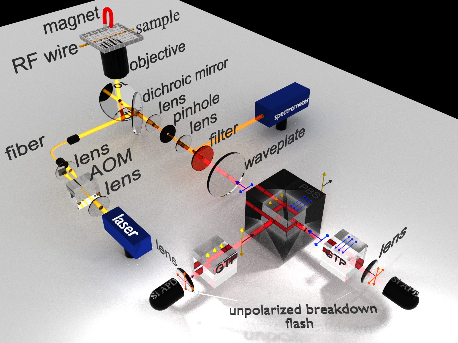
Figure 1.12: Experimental setup. The excitation beam (orange) is focused with an oil objective on the sample. The fluorescent light from silicon vacancy centers (red) passes the dichroic mirror while laser light is blocked. To suppress background emission the light is passed through a pinhole in the focus of two lenses (confocal configuration). This light is filtered by 800 nm longpass filter and sent to the spectrometer or 905 nm lp filter and sent to the detection path toward apds. The usual 50:50 bs before the apds is replaced with a pbs and a half-wave plate is placed before the pbs. The half wave plate is adjusted such that the fluorescent intensities detected by each apd become even. The blocking of the breakdown emissions from Si apds is achieved by using both gtp before the apds and the pbs. The breakdown flash from the apds polarized either parallel or perpendicular to the optics table by the gtps cannot enter the path to the other apds due the combination of pbs and a different orientated gtp. For a more detailed description see main text.
The collimated laser-beam is sent using 2 mirrors on a lens, an aom is placed in the focal point of the lens (aom EQ Photonic 3200-124). Because the aom acts as an optical grating, the laser light is essentially split into different diffraction orders.
To separate the diffraction orders, an iris is placed in a way that only the first order is transmitted, whereas all other are blocked. The optical alignment is made in a way, that very high on/off ratios and fast rise-times (typically around 15 ns) are achieved. The aom allows to adjust laser intensity by tuning the aom driving power, and more importantly for switching the CW laser on and off in order to perform pulsed measurements.
The second lens, placed after the aom is used to collimate the laser beam, which is then sent through another mirror into a photonic crystal fiber. The photonic crystal fiber transmits light in a wide wave-length ranges, and is mainly used to create an again collimated Gaussian beam profile using an objective for outcoupling. Another benefit of the fiber is the possibility to change the excitation part without disturbing the microscope and detection-path. In order to remove unwanted fluorescence, a laser cleanup filter (730/10 nm) can be placed after the fiber out-coupler.
After the fiber out-coupler a wave-plate and a pbs is added. The angle of the wave-plate is set in a way that the transmission is maximized through the PBS. That ensures well linear polarized light. The polarization can then be changed using a motorized stage (M101, LK-instruments) with 0.3° resolution, which is placed after the dichroic long-pass mirror. The dichroic mirror basically reflects the laser-beam towards the 45° mirror, whereas the fluorescence can be transmitted.
Nano-positioning Stage System
The path of the microscope is illustrated in Figure 1.12. The beam is focused onto the SiC sample by an oil immersion lens (Olympus UPlanSapo, 60x, NA 1.35). The objective can be moved to laser scan the sample, and allows for precise addressing of single emitters. The movement is performed using a 3D piezo scanner (Physikalische Instrumente). In order to drive the electron spins, RF signal are provided though a home-built sample holder, where a 20 µm thick copper wire serves as a waveguide, as shown in Figure 1.12.
Detection Path
In order to detect the fluorescence emitted by the defect, the same objective as in the excitation path is used. Typically not only the point like defects are excited, but also it’s surrounding material, as described by the psf. The psf is from ellipsoidal form, where the lateral dimension can be calculated via , and the axial direction by (Webb, 1996). With a typical refractive index for the immersion oil used and nm the excitation wavelength. The psf has nm and nm. The resulting confocal volume is of the order 1.55 fL.
As before mentioned the fluorescence light is collected by the same objective and directed therefore backwards to the dichroic mirror. The red-shifted fluorescence light is transmitted through the dichroic mirror, whereas the laser light is partially reflected back towards the fiber. In order to further suppress the background signal the fluorescence is focused onto a 50 µm-sized pinhole which acts as a spatial filter. Subsequently the light from the pinhole is collimated by another lens. Additional to the spatial filtering, a spectral filtering is performed by a 905 nm long-pass filter to remove residual backscattered laser light, which was not blocked by the dichroic. Consecutively, the filtered and collimated fluorescence is traveling through another wave-plate, combined with a subsequent pbs allows for polarization measurements in detection. Hence, the fluorescence light is split depending on the polarization into two perpendicular beams and pass the gtps. Each beam is then focused on an individual apd (Exelitas, SPCM-AQRH-15).
Electronic Supply and Software
The experimental apparatus is connected to a computer via a specialized measurement card from National Instruments with several options for analog and digital input and output lines. The card can be fully controlled with a self-written Python program based on a formerly developed software called pi3diamond for the investigation of color centers in diamond. The program allows for confocal imaging, and for electron/nuclear spin control.
A confocal scan is performed by moving the objective over the sample with the 3D-piezo stage, whose movement is controlled by 3 analog output ports from the NI-card. The scan-limits (x,y,z) are given by the stage and allow for scans in the range of (100×100×10) µm³. The fluorescence signal collected by the apds is sent to a fpga, whose software was developed in-house. The fpga allows for single photon counting in the sub nano-second regime. Because the data-rate is limited by the USB-type-2-connection, the photons can be binned inside the fpga and its result delivered to the computer. The software plots the fluorescence intensity as a function of two arbitrary chosen spatial dimensions. A depth scan can be performed by fixing either or -axis. An in-plane scan can be performed by fixing -direction.
Radio-frequency control
In order to manipulate single V-spins, rf-waves are generated by a vector signal generator (SMIQ, Rhode & Schwarz), whose frequency output can be controlled by the software. The SMIQ is operated in the cw-mode, additional pulsing is achieved with the help of electronic switches (Minicircuits), connected to the rf output-port of the SMIQ. Pulse control is achieved with a pulse generator, which is based on a similar fpga as for the photon counting module, but running a different hardware kernel. The software allows for controlling the pulse generator as well. Subsequently the RF-signal is amplified (Minicircuits, ZHL-42W), and applied to the sample-holder. A 50 µm-wire is used as rf antenna. Finally, the rf-signal is damped with a 30 dB attenuator, before terminated with a 50 Ω resistor to the ground plate of the sample holder. Instead of dumping the signal into the resistor, it can be plugged into an oscilloscope to monitor the signal.
Magnetic field alignment
In order to lift the degeneracy of magnetic Zeeman-sublevels a magnetic field needs to be applied along the symmetry axis of the vsi defect. Magnetic field alignment is performed by a 3D motorized linear stage (Standa) with a resolution of 0.01 mm. An USB interface connects its control-unit to the computer, and allows for remote movements. Thus, an automated alignment algorithm can be used to adjust the magnetic field parallel to the symmetry axis of the spin defect. Depending on the growth-technique (on-axis, or 4°), all the silicon vacancy defects are oriented in that direction, which is around the -axis.

Figure 1.13: Magnetic field alignment. Numerically solved transitions for -system with an external magnetic field 144 MHz.
The magnet is mounted in a way that it approaches the sample from top. Because the magneto-optical effect is not very high, in terms of fluorescence change due to spin-mixing, the fluorescence intensity cannot directly be used to align the magnetic field. Instead, an odmr-measurement needs to be performed where the splitting is monitored. Once the splitting is maximized to 140 MHz () the alignment is achieved (see Figure 1.13).